Ceramic PCBs, also known as ceramic substrates or ceramic laminates, differ from traditional PCBs made of organic materials like fiberglass and epoxy resin. They are produced through a specialized process that directly bonds copper foil to the surface of a substrate made of aluminum oxide (Al₂O₃), aluminum nitride (AlN), or other ceramic materials.
Unlike conventional FR-4 (fiberglass) materials, ceramic substrates exhibit superior high-frequency and electrical properties. They possess not only high thermal conductivity but also exceptional chemical and thermal stability—characteristics unmatched by traditional organic substrates. Consequently, ceramic materials have become the ideal packaging choice for next-generation large-scale integrated circuits and power electronic modules.
Key Advantages:
- Higher thermal conductivity
- Better thermal expansion coefficient matching
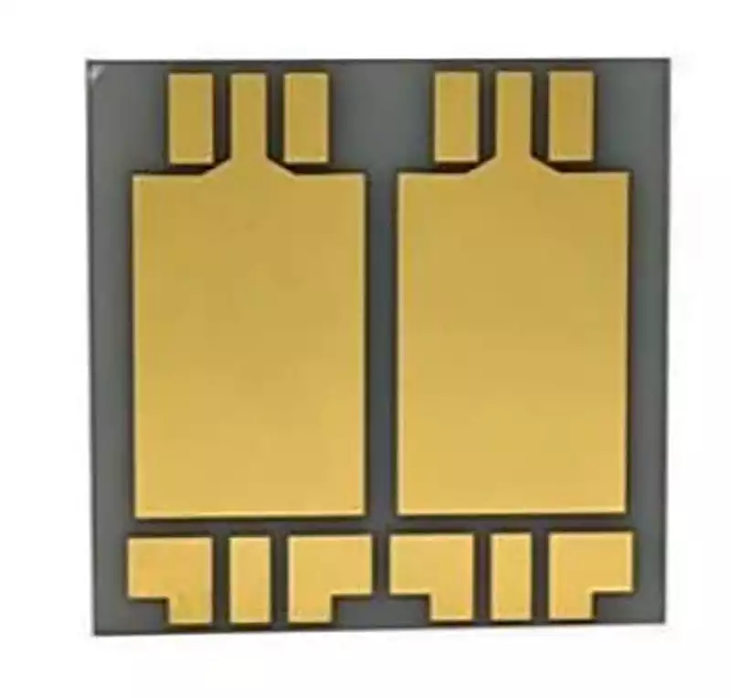
- Stronger, lower-resistance metal film layers on aluminum oxide ceramic circuit boards
- Excellent solderability and high operating temperature tolerance
- Superior insulation properties
- Low high-frequency loss
- Capable of high-density assembly
- Free of organic components, resistant to cosmic radiation, offering high reliability and extended service life in aerospace applications
- Copper layers free of oxide layers, enabling long-term operation in reducing atmospheres
Key Technologies in Ceramic Substrate Manufacturing Processes:
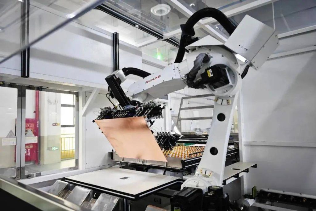
- Drilling: Utilizing mechanical drilling methods to establish interconnecting pathways between metal layers.
- Plated Through-Hole (PTH) Plating: After drilling copper interconnects between layers, the circuitry remains non-conductive. Therefore, a conductive layer must be formed on the hole walls to achieve electrical continuity—a process commonly referred to as the “PTH process” within the industry. This process primarily encompasses three steps: stripping of resist residue, electroless copper plating, and electrolytic copper plating.
- Dry Film Laminating: Used to create photosensitive etch resist layers.
- Inner Layer Pattern Transfer: Transfers the image from the master film onto the board surface through exposure.
- Outer Layer Circuit Exposure: After applying photosensitive film, the PCB undergoes a process similar to inner layer fabrication, involving re-exposure and development. The primary function of this photosensitive film is to delineate areas requiring electroplating versus those exempt from plating, with the covered regions designated as non-plating zones.
- Magnetron Sputtering: Utilizes energy and momentum transfer between positive ions generated during gas glow discharge and atoms on the target material surface to deposit substances from the source material onto the substrate, achieving thin-film deposition.
- Etching—External Circuit Formation: A technique removing material through chemical reactions or physical impact. Etching selectively removes material according to specific patterns. After circuit plating is complete, the circuit board is sent to a stripping, etching, and tin line removal machine. Its primary task is to completely remove the plating resist, exposing the copper to be etched to the etchant. Since the top of the circuit area is protected by tin, an alkaline etchant is used to etch the copper. The circuit area, protected by tin, remains intact, ultimately revealing the entire circuit pattern on the board surface.
- Solder Mask Application: Ceramic PCBs primarily serve to mount electronic components and facilitate connections. After circuit formation, assembly areas must be clearly defined, with non-assembly regions protected by polymeric materials. Since solder is used for component assembly and connection, this polymeric protective coating is termed “solder mask.” Currently, most photosensitive solder resist employs wet ink printing methods.
Primary Applications of Ceramic PCBs:
- High-Power Power Semiconductor Modules:
Semiconductor cooling devices and electronic heating elements: Due to their exceptional thermal dissipation capabilities, ceramic PCBs serve as an ideal material for semiconductor coolers (e.g., devices based on the Peltier effect) and electronic heaters. These devices rely on efficient thermal management to ensure stable performance. Power Control Circuits and Power Integrated Hybrid Circuits: In high-power applications like power control circuits and power integrated hybrid circuits, ceramic PCBs effectively manage thermal loads through their high thermal conductivity, thereby safeguarding circuit reliability and longevity. - Smart Power Components:
High-Frequency Switching Power Supply Applications: Ceramic PCBs serve as ideal materials for high-frequency switching power supplies due to their low dielectric loss and high thermal conductivity. These power supplies demand superior thermal management and signal integrity during high-frequency operation—requirements precisely met by ceramic PCBs.
Solid-State Relay Applications: For solid-state relays, ceramic PCBs’ exceptional thermal conductivity facilitates rapid heat dissipation. This property ensures stable and reliable performance even during prolonged high-load operation.
- Automotive Electronics, Aerospace, and Military Components:
Automotive Electronics: Within automotive electronics, ceramic PCBs are used in engine control units, sensors, and other critical electronic components. Their outstanding high-temperature resistance and vibration tolerance make them exceptionally well-suited for the harsh operating environments encountered in vehicles.
Aerospace and Military Electronics: In aerospace and military electronics, ceramic PCBs are extensively used in critical electronic components due to their superior high-temperature resistance, corrosion resistance, and radiation resistance. This ensures reliable operation of these components under extreme conditions.
- Solar Panel Assemblies:
Telecommunications Switches and Receiving Systems: Ceramic PCBs enhance efficiency and reliability in solar panels and telecommunications equipment by leveraging their superior thermal conductivity and insulation properties. Industrial Electronics like Lasers: In lasers and other industrial electronics, ceramic PCBs’ high temperature resistance and heat dissipation capabilities support stable operation of high-power lasers and industrial equipment. - High-Power LED Lighting:
High-Power LED Lighting: Ceramic PCBs serve as a critical material for high-power LED lighting. Their superior thermal conductivity facilitates rapid heat dissipation in LED fixtures, extending service life and enhancing luminous efficiency.