
What Is FR-4 PCB Material and How Is It Used?
FR-4 PCB material is a glass-reinforced epoxy laminate widely used as the insulating substrate in rigid printed circuit boards. It combines woven glass fiber reinforcement with an epoxy resin system
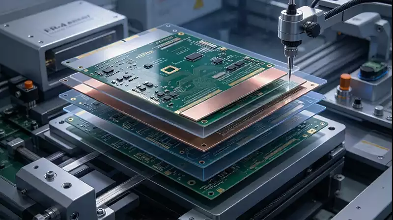
FR-4 PCB material is a glass-reinforced epoxy laminate widely used as the insulating substrate in rigid printed circuit boards. It combines woven glass fiber reinforcement with an epoxy resin system
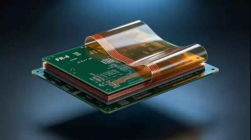
A rigid flex PCB integrates rigid and flexible sections in one laminated structure. This guide covers IPC-2223 design rules, materials and bend radii.
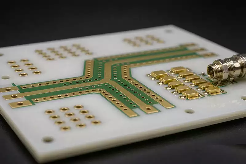
A microwave RF PCB is a specialized printed circuit board designed for high-frequency signal transmission. It serves as a critical component in advanced applications such as 5G communication infrastructure, satellite
Microwave RF PCB Design and Manufacturing Guidelines Read More »
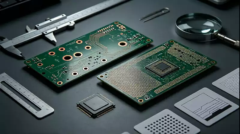
An HDI PCB and a standard multilayer PCB can use exactly the same schematic and perform the same basic electrical functions, yet they may not be equally suitable for a
How HDI PCBs Compare with Standard Multilayer PCBs Read More »
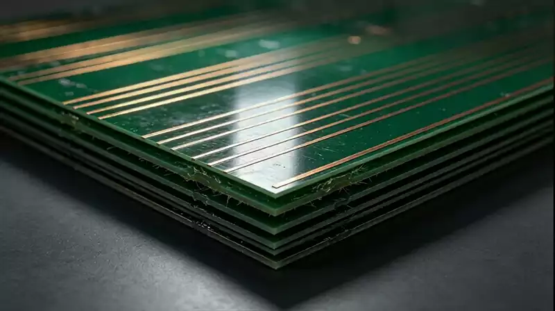
A PCB stackup defines the vertical structure of a printed circuit board and determines how copper layers and dielectric materials are arranged, separated, and laminated to form the finished board.
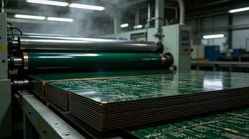
PCB board fabrication is the set of manufacturing steps that turns a digital design package into a bare, unpopulated printed circuit board. It is the part of the supply chain
How PCB Board Fabrication Works From Design Data to a Finished Board Read More »
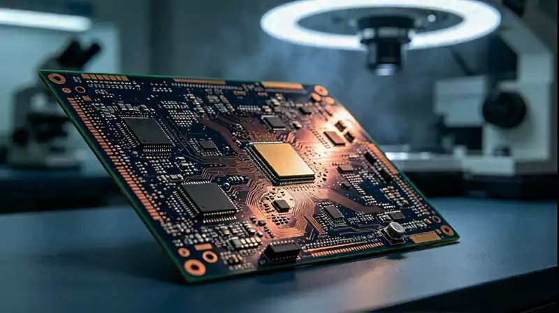
Choosing an hdi pcb stackup is the decision that quietly sets your cost, lead time, and yield before a single trace is drawn. The notation 1+N+1, 2+N+2 and any-layer looks
What HDI PCB Stackup Does Your Design Need 1+N+1 2+N+2 or Any Layer Read More »

HDI PCB cost is driven by sequential lamination cycles, microvia stacking and fine-line geometry. See real 2026 price ranges by build-up and quantity.

HDI PCB manufacturing builds boards through repeated laser drilling, plating and sequential lamination cycles. See the full process and its quality limits.
The Core Process of Modern HDI PCB Manufacturing Read More »

An HDI PCB packs more interconnect into less board area using laser-drilled microvias, blind and buried vias, and sequential lamination. Here is how it works.
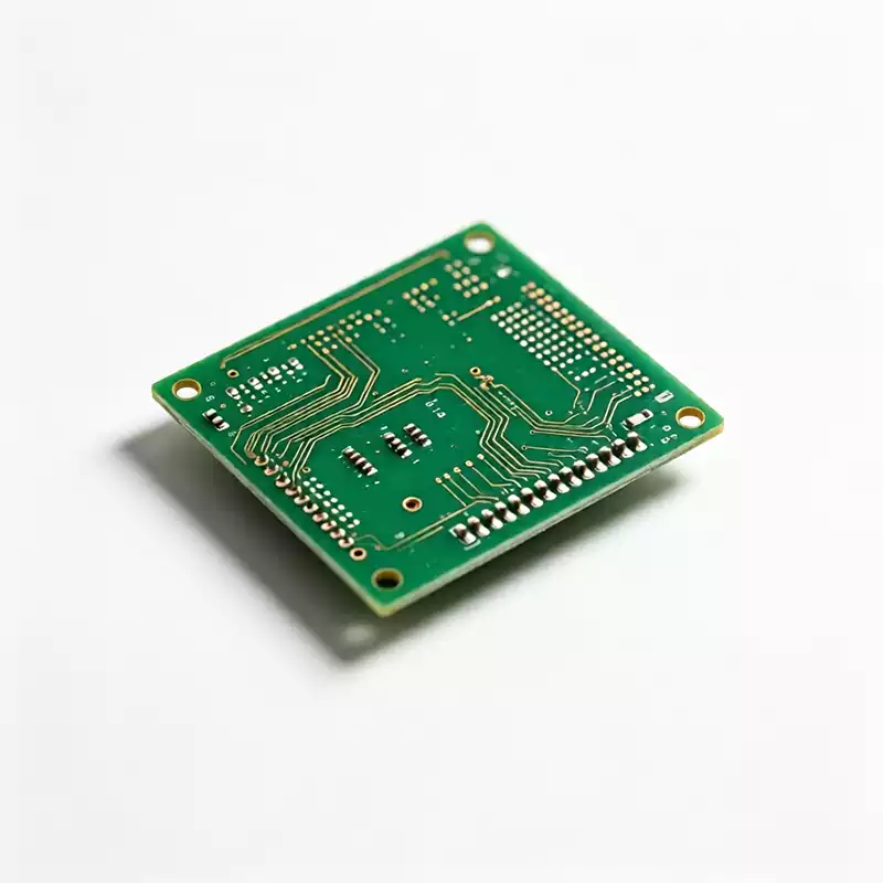
1 layer PCB, also known as single‑sided PCB, represents the most basic form of printed circuit board. Conductive copper foil exists only on one side of the dielectric substrate, and
1 Layer PCB Structure Process and Practical Application Read More »