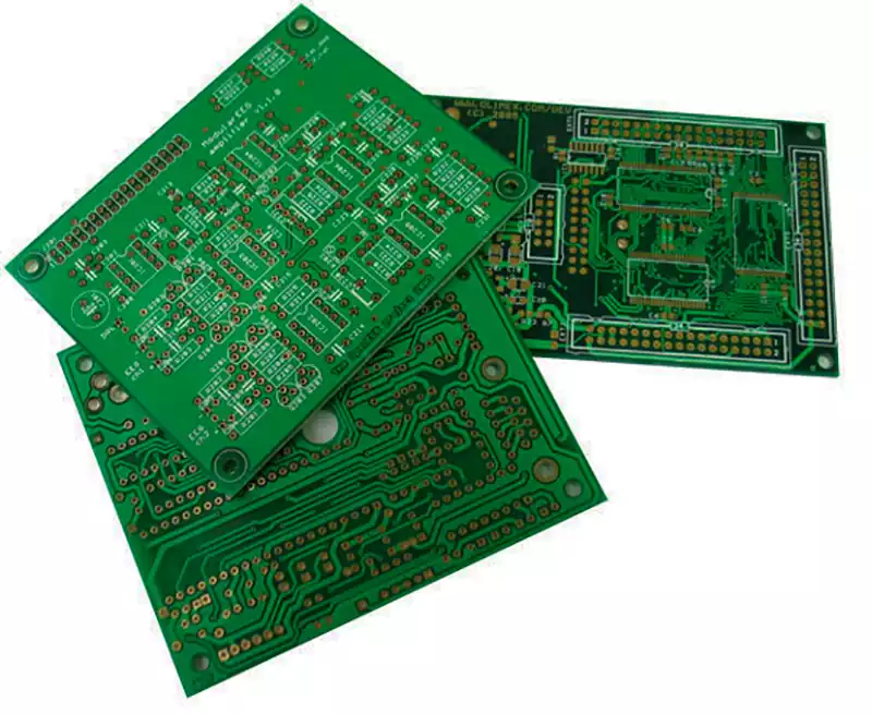
A single sided PCB, also known simply as a single sided PCB board or single layer pcb, refers to a printed circuit board on which conductive copper foil circuits and pads are formed on only one side of the insulating substrate. Within the broad family of printed circuit boards, the single sided pcbhas the simplest structure. Generally, electronic components are mounted on the side without copper foil, whilst the copper foil circuits and solder pads are located on the opposite side.
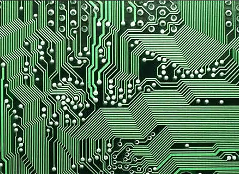
Single sided pcb are coated with copper foil on only one side of the substrate, and all routing must be completed on the same side. As the traces cannot cross, layout design is subject to significant constraints, often requiring the use of jumpers or routing around obstacles to achieve connections. The typical manufacturing process includes pattern transfer, etching and wave soldering. Due to their simple structure and lower cost, these pcb boards are widely used in power adapters, LED lighting, home appliance control boards and consumer electronics.
Single sided pcb have copper foil applied to only one side of the substrate to form conductive patterns; all components are mounted on this side, with the traces distributed on the same side, whilst the other side has no conductive patterns.
Taking a common 1.6 mm thick single sided pcbs an example, its typical structure comprises a top copper foil trace layer, an FR-4 epoxy glass fibre substrate, a solder mask protective layer, and a silkscreen character layer.
The manufacturing material for single sided pcb uses copper-clad laminate as the substrate. Common types and compositions are as follows:
FR-4 (Glass Fibre Epoxy Resin Board)
This uses glass fibre cloth as the reinforcing material and epoxy resin as the insulating binder, with a single layer of copper foil applied to the surface to form the conductive layer. It is characterised by low cost, high mechanical strength and good heat resistance, making it the most widely used type, commonly found in household appliances and basic electronic equipment.
Phenolic Paper Substrate (FR-1 / FR-2)
These use cellulose paper as the insulating substrate and phenolic resin as the binder, with copper cladding on one side. Their greatest advantage is their extremely low cost, though they have poor heat resistance and mechanical strength. They are primarily used in low-end consumer electronics such as toys and simple remote controls.
Aluminium Substrates (Metal Substrates)
Structurally, they consist of an aluminium plate (heat dissipation layer), an insulating dielectric layer and a single-sided copper foil, in that order. They offer excellent heat dissipation and are suitable for applications requiring effective heat management, such as LED lighting and power modules.
In addition,single layer pcbs include the following essential components:
Copper foil: Used as the conductive layer, typically with a thickness of 18μm to 35μm.
Solder mask (green ink): Applied to non-soldering areas to prevent oxidation and provide insulation.
Silkscreen layer: Used to mark component positions and parameter information.
Manufacturing process for single sided pcb:
Single sided pcb are primarily manufactured using the subtractive process. Specifically, a layer of photoresist is first applied to the surface of the copper-clad laminate; through exposure and development, the circuit pattern is precisely transferred onto the copper surface. Subsequently, a chemical etching solution is used to remove the copper foil not protected by the photoresist, and finally, the photoresist is stripped away, thereby forming the required circuit.
The production process for single sided pcb is relatively straightforward and primarily comprises the following stages:
First, the copper-clad laminate is cut into suitable smaller sheets according to the design dimensions. Next, the pattern transfer step is carried out: a photosensitive dry film or wet film is evenly applied to the copper foil surface, and exposure is performed using a photomask or direct imaging (LDI) technology. The unexposed areas dissolve in the developer, thereby exposing the copper surface.
This is followed by the etching process, where the PCB is immersed in an acidic etchant to remove the copper foil not covered by the resist, thereby forming the circuit pattern. Once etching is complete, the residual resist is removed. Typically, the drilling process is carried out after etching to create mounting holes for components and positioning holes. Due to the nature of single sided pcb, metallisation is not required after drilling. This is followed by solder mask application and screen printing: first, the solder mask ink is applied; then, exposure and development are used to expose the pads; finally, component part numbers and polarity markings are printed. After surface treatment and contour cutting, a single sided pcbis complete.
With regard to surface treatment, single sided pcb generally require surface treatment to prevent oxidation of the copper pads during storage and assembly, and to improve their solderability. Hot Air Leveling (HASL) is a more traditional process, in which the PCB is immersed in molten solder and then blown flat with hot air, thereby forming a uniform layer of tin-lead alloy on the surface. This process offers the advantages of low cost and good solderability, making it suitable for high-current applications and through-hole components; however, its surface flatness is somewhat lacking.
The Organic Solder Preservative (OSP) process, on the other hand, creates an organic protective layer on the copper surface. It is a simple, low-cost process that produces a flat surface, making it suitable for surface-mount components, although its scratch resistance is relatively poor. For precision components requiring extremely high surface flatness, the electrochemical nickel-gold plating (ENIG) process may be employed, which involves first plating a layer of nickel onto the copper surface, followed by a layer of gold. This process offers excellent oxidation resistance but is relatively costly.
Key Points for single sided pcb design
In single sided pcb design, a rational layout is the key to success. The sequence of ‘layout first, routing second’ should be followed; components should be placed in accordance with the signal flow shown in the schematic diagram, and component positioning, orientation and package types should be adjusted to minimise trace crossings as much as possible. At the same time, the positioning of connectors must be considered, and functional modules should be zoned; components should be arranged compactly whilst ensuring safe clearances, leaving sufficient space for subsequent routing.
The fundamental requirement for single sided pcb design is that all conductors must be connected within the same copper layer and must not cross one another. For unavoidable cross-connections, jumpers must be used; the number of jumpers should be minimised, and they should be arranged in a centralised and orderly manner, whilst being clearly labelled on the silkscreen layer. When routing, signal lines should utilise 45° angles or curved transitions to avoid sharp angles and right angles, whilst adhering to the principle of the shortest path.
Power and ground traces should be appropriately widened to carry higher currents and reduce trace impedance. It is recommended to lay out the ground network first, using large copper pads wherever possible to reduce noise and provide shielding. For sensitive circuits, a star or single-point grounding configuration may be adopted.
Pad dimensions must exceed the diameter of the component leads to ensure good solderability, and traces should connect smoothly to the centre or side of the pad. During design, the manufacturer’s process specifications must be strictly adhered to. Clear silkscreen markings should be added, and teardrops should be included at the connection points between traces and pads to enhance mechanical strength.
When designing single sided pcb using software such as Altium Designer, all routing should be confined to a single layer, with the other layer disabled. The recommended design workflow is as follows: after creating the component library, begin with careful component placement; then route critical signal lines first, followed by standard signal lines; after handling jumpers, perform routing optimisation and copper fill; finally, add the silkscreen layer and run a Design Rule Check (DRC).
Advantages and Disadvantages of single sided pcb
Advantages of single sided pcb:
Single sided pcb require fewer raw materials and are therefore less expensive;
The manufacturing process involves fewer steps, resulting in a shorter overall production time;
The design and structure of the circuit are relatively simple, so the design can be completed without extensive professional experience;
Due to the simplicity of the manufacturing process, for high-volume orders, the larger the order quantity, the more favourable the price.
On the other hand, when compared to double-sided or multi-layer boards of the same size, the disadvantages of single sided pcb continue to limit their development:
The limited surface area of single sided pcb cannot meet the requirements for installing a large number of components or accommodating more traces; furthermore, if too many components are mounted, this may result in slow connection speeds and power loss, thus severely limiting the range of product applications.