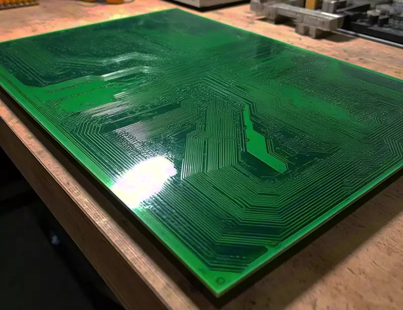
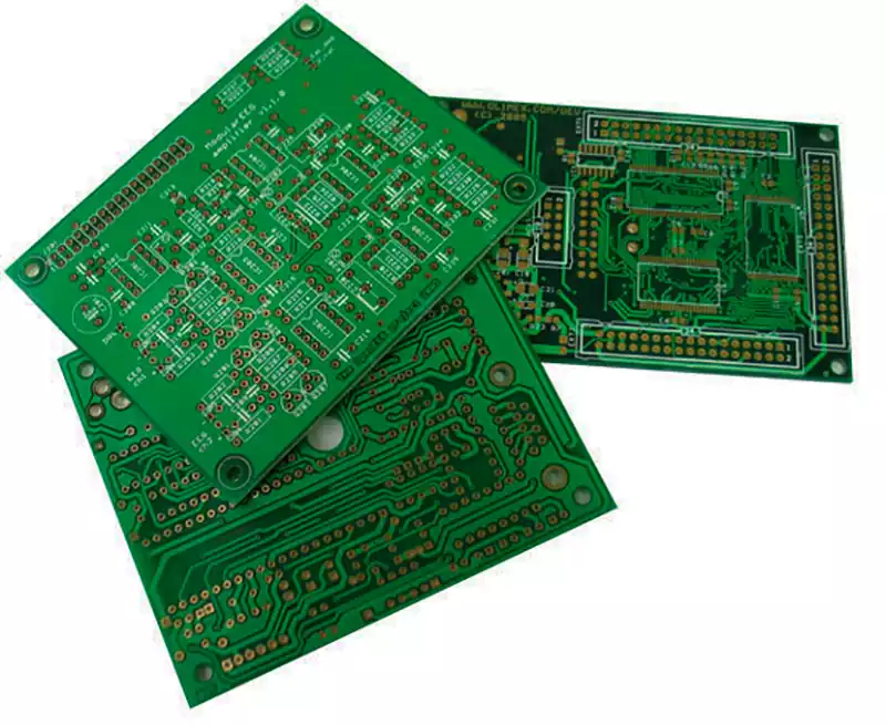
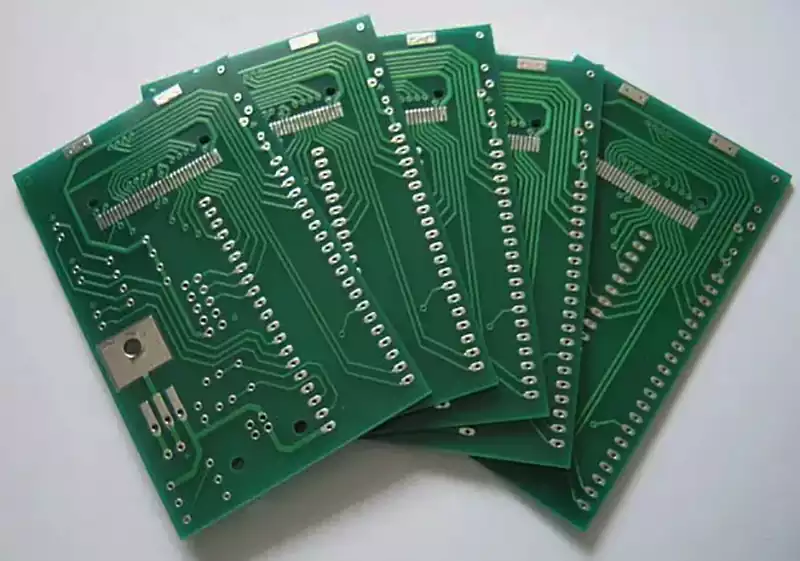
Solar panel PCB board serves as core photoelectric conversion components within the new energy sector. These devices directly convert light energy into electric energy by leveraging the photoelectric properties of semiconductors and constitute the fundamental building blocks of all solar photovoltaic power generation systems.
As a vital carrier for the deployment of clean and renewable energy, photovoltaic panels integrated with solar panel PCB board substrates are widely deployed across a broad spectrum of applications including residential distributed power generation, commercial centralized power supply, outdoor energy storage hardware and industrial photovoltaic power stations. Characterized by zero pollutant emissions and sustainable power generation capabilities, they stand as pivotal equipment that facilitates the transformation of global energy structures and advances the development of a low-carbon green economy.
The fundamental power-generating unit of a photovoltaic panel fitted with solar panel PCB board backplates is the solar cell chip, with silicon-based materials dominating raw material selections for mainstream chips in the current industry landscape. Its power-generating architecture is constructed using two differently doped silicon semiconductor layers: n-type silicon semiconductors formed via phosphorus doping and p-type silicon semiconductors manufactured through boron doping. When these two semiconductor layers with distinct electrical properties are tightly bonded together, a PN junction spontaneously forms at their contact interface, a structure that acts as the foundational mechanism enabling photoelectric conversion and stable current transmission through circuit traces.
The power generation performance of solar panels relies entirely on the photovoltaic effect, a physical photoconversion phenomenon exclusive to semiconductor materials. Silicon, germanium and other high-performance semiconductor substrates are predominantly adopted for core cell chips; under natural sunlight illumination, photons contained within solar rays interact with atomic structures inside semiconductors, exciting bound electrons to break free and form free electrons paired with corresponding holes, which together generate charge carriers capable of directional migration.
Driven by the built-in electric field originating from the PN junction, free electrons and holes undergo directional separation and orderly displacement to continuously generate steady photocurrent. This current is channelled outward through embedded conductive traces integrated into the solar panel PCB board assembly, ultimately producing usable electrical energy and completing the lossless conversion of light energy to electric power.
The power output of photovoltaic panels is instantaneous, meaning electricity generated under sufficient illumination cannot be stored in large volumes directly. For this reason, a complete photovoltaic system must incorporate charge control modules to facilitate energy storage and hardware protection, with charge controllers functioning as core voltage regulation and protection components that monitor real-time state of charge, input current and voltage parameters of connected energy storage batteries, matching the power transmission limits of solar panel PCB board circuits.
During daylight hours with ample sunlight, panels sustain continuous photoelectric power generation; electricity passes through voltage regulation and rectification processes carried out by the controller, with a portion of the power directly supplying connected external loads and surplus energy routed to attached battery energy storage packs. Meanwhile, the controller intelligently modulates charging power to eliminate risks such as overcharging, over-discharging and overcurrent conditions that may damage circuit wiring, comprehensively safeguarding the operational safety and service lifespan of storage batteries and the integrated solar panel PCB board.
Raw power output from photovoltaic panels takes the form of direct current, while the vast majority of residential electrical appliances and industrial terminal loads operate on alternating current, creating an inherent mismatch in power supply formats. This makes inverters indispensable core matching hardware within photovoltaic power supply systems paired with solar panel PCB board assemblies.
Inverters precisely adjust current polarity, power frequency and voltage amplitude, converting low-voltage direct current produced by PV panels into alternating current compliant with residential and industrial electrical standards to accommodate the power demands of diverse electrical equipment and achieve efficient, compliant utilisation of electricity transmitted via circuit traces.
Photovoltaic power generation is heavily reliant on natural sunlight, rendering panels incapable of normal power output during nighttime, heavy rainfall, haze and other low-light or zero-light conditions. To maintain consistent, stable power delivery, full photovoltaic systems are equipped with dedicated battery energy storage packs that reserve excess photovoltaic power generated during daylight hours and deliver consistent power flow compatible with solar panel PCB board load limits.
These packs automatically switch to discharge mode under low or no illumination to sustain power supply for connected loads, while integrated intelligent control units precisely regulate charge and discharge cycles to prevent long-term undercharging and performance degradation caused by overcharging, significantly boosting the overall operational stability of the complete photovoltaic system built around circuit substrates.
Multiple functional layers make up the full structure of solar panels, starting with surface encapsulation materials whose primary function is to encapsulate and protect internal cell chips, shielding them from external damage caused by sand, rainwater and ultraviolet radiation while maximising light transmittance to preserve photoelectric conversion efficiency.
Three mainstream material options prevail across the industry: tempered glass, ethylene-tetrafluoroethylene copolymer abbreviated as ETFE and polyethylene terephthalate abbreviated as PET. Tempered glass represents a traditional high-end encapsulation material delivering high light transmittance, exceptional weather resistance, robust mechanical strength and stable chemical properties with a service life exceeding 20 years, its key drawbacks being excessive self-weight, limited impact toughness and elevated manufacturing costs that indirectly raise the production expense of matched solar panel PCB board.
ETFE, a novel premium polymeric encapsulation material, matches glass in light transmission performance while offering lightweight construction, superior flexibility, self-cleaning functionality and strong anti-ageing characteristics, making it suitable for flexible photovoltaic panels and precision outdoor equipment assembled with thin-type circuit substrates, though it carries a high price tag and insufficient compressive mechanical strength.
PET functions as an economical encapsulation material featuring low production costs, lightweight construction and straightforward processing workflows with light transmittance meeting basic operational requirements, and sees widespread use in low-power miniature photovoltaic products paired with entry-level solar panel PCB board; its major limitation lies in subpar weather resistance that leads to accelerated performance attenuation and shortened service life after prolonged outdoor exposure, causing premature ageing of attached circuit substrates.
Adhesive film layers serve to bond and secure surface encapsulation materials, core cell wafers and rear backsheets, while delivering sealed waterproofing, electrical insulation and compressive buffering performance to guard circuit traces. As a critical layer that stabilises panel structure and slows power attenuation transmitted through conductive paths, the industry primarily employs ethylene vinyl acetate films known as EVA films and polyolefin elastomer films known as POE films.
EVA films boast mature production technology, cost-effective performance, high light transmittance, strong adhesive bonding and reliable resistance to thermal-humidity ageing, rendering them compatible with most standard photovoltaic modules assembled with conventional solar panel PCB board.
Nevertheless, this material exhibits high water vapour transmission rates, with long-term service prone to hydrolysis issues that trigger potential risks including potential induced degradation, or PID, and reduced light reflection efficiency that cuts down the power transfer efficiency of circuit boards. POE films classify as high-performance functional films that outperform EVA films in water vapour barrier capacity, electrical insulation and anti-PID performance, making them ideal for dual-glass modules and high-efficiency n-type solar cells matched with high-reliability solar panel PCB board. Their disadvantages stem from stringent processing specifications that create manufacturing defects such as internal air bubbles and interlayer slippage during production, alongside higher raw material and fabrication expenses for both film and supporting circuit substrates.
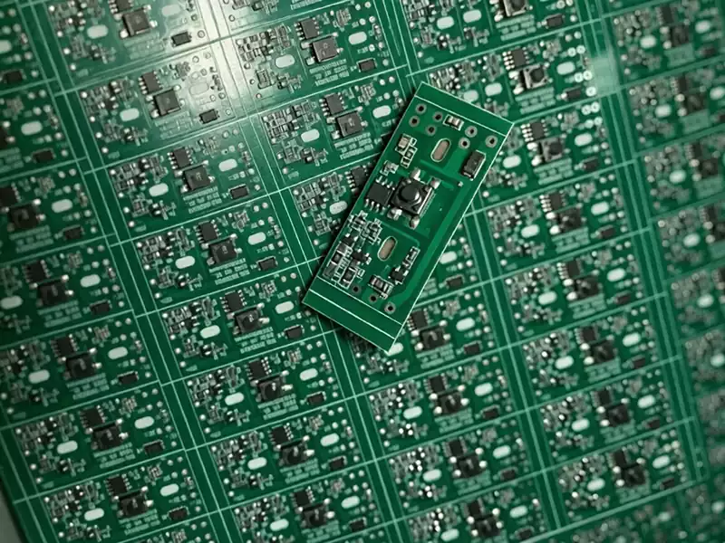
Cell wafers constitute the power-generating core of photovoltaic panels and directly determine the photoelectric conversion efficiency and overall power throughput of finished devices, with three mainstream industrial classifications including monocrystalline silicon wafers, polycrystalline silicon wafers and thin-film cell wafers. Monocrystalline silicon wafers are manufactured from high-purity monocrystalline silicon ingots through precision processes including cutting, texturing, cleaning and doping, delivering high photoelectric conversion efficiency, stable long-term operation and extended service life as the preferred solution for high-efficiency photovoltaic power stations paired with heavy-duty solar panel PCB board, with elevated raw material and processing costs as their sole downside.
Polycrystalline silicon wafers feature simplified production workflows and low manufacturing costs with outstanding mass production cost performance, commonly adopted for small and medium-sized photovoltaic hardware fitted with standard circuit substrates despite slightly lower conversion efficiency and moderate overall performance compared to monocrystalline alternatives.
Thin-film cell wafers represent an emerging lightweight chip category encompassing amorphous silicon, copper indium gallium diselenide and cadmium telluride variants, distinguished by ultra-thin form factors, flexible bendability and compatibility with large-area substrate lamination to fit irregular-shaped and portable photovoltaic devices using flexible circuit substrates, yet constrained by relatively low conversion efficiency and room for improvement in long-term operational stability of thin assembly structures.
Rear backsheet structures deliver electrical insulation protection, circuit interconnection and mechanical structural support for full photovoltaic panels. Small portable photovoltaic panels typically utilise standard printed circuit boards as backsheets with streamlined integrated circuit traces and broad compatibility, while large industrial-grade photovoltaic modules abandon thin lightweight board architectures and adopt dedicated copper strips and high-temperature resistant adhesive tapes to complete series and parallel interconnection of cell wafers, ensuring safe operation under high-current and high-power operating conditions that exceed the load capacity of ordinary solar panel PCB board.
A set of standard performance metrics quantifies the functional capacity of solar panels, starting with conversion efficiency, defined as the rate at which cell wafers transform solar energy into electrical power flowing through conductive traces and acting as a core benchmark for evaluating wafer and matching board performance. Current industry figures place monocrystalline silicon wafer conversion efficiency above 20%, polycrystalline silicon wafer efficiency between 15% and 20%, and thin-film wafer efficiency at a relatively lower range of 10% to 15%, which directly affects the current output requirement of supporting solar panel PCB board.
Maximum power output refers to the peak power a cell wafer can generate under standard test conditions, including an irradiance level of 1000 watts per square metre or 38,000 lux simulated light, a cell temperature of 25 degrees Celsius and an AM1.5 standard spectral distribution, parameters that engineers reference to design the trace width and copper thickness of circuit substrates.
Open-circuit voltage denotes the voltage measured across an unloaded cell wafer with no external circuit connection, a critical parameter that reflects the magnitude and distribution of the internal electric field within the wafer and guides the layer stack design of circuit boards. Short-circuit current describes the current generated when the positive and negative terminals of a cell wafer are directly connected, representing the maximum output current achievable and indicating the wafer’s capacity to generate electron-hole pairs that determine the current carrying capacity of solar panel PCB board.
Nominal operating voltage and nominal operating current correspond respectively to the voltage and current values measured at the maximum power point of the cell wafer, core parameters for sizing conductive traces on custom circuit substrates.
Structural design of solar panels follows two core engineering frameworks covering area-power matching and voltage series-parallel matching, both critical for reliable board manufacturing. The effective light-receiving area of a photovoltaic panel directly dictates its rated power output, requiring precise calculations that integrate target power ratings, photoelectric conversion efficiency and standard irradiance levels during design stages via the universally accepted industry formula A=P/(η×G), where P stands for the panel’s rated output power, η represents the photoelectric conversion efficiency of the cell chip and G denotes ambient irradiance with the standard test irradiance set at 1000 watts per square metre, all data used to customize the layout of solar panel PCB board.
As a practical illustration, a 1-watt photovoltaic panel with 20% conversion efficiency requires a light-receiving area of 0.005 square metres under standard operating conditions, corresponding to physical dimensions of approximately 10 centimetres by 5 centimetres, a dimension standard for miniature circuit substrates.
This calculation framework accurately aligns physical panel dimensions with power generation targets to eliminate excess surface area or insufficient power output, supporting product development for all types of terminal hardware and tailored board solutions. A single solar cell wafer delivers a nominal operating voltage of roughly 0.55 volts and an open-circuit voltage ranging from 0.65 volts to 0.7 volts, a voltage level insufficient to meet power supply requirements for most conventional equipment, which drives the series-parallel layout design of circuit substrates.
Practical design workflows adhere to the principle of series connection for voltage elevation followed by parallel connection for current amplification: multiple cell wafers are wired in series to boost overall output voltage, then grouped in parallel to raise total output current, a circuit layout fully implemented on solar panel PCB board. For a standard 5-volt power supply system, nine to ten cell wafers wired in series achieve matching voltage levels, with additional parallel strings added to scale current capacity according to load requirements, all routed through custom conductive traces.
Solar panels assembled with circuit substrates carry distinct advantages alongside inherent limitations in industrial deployment. Their primary strengths include exceptional photoelectric conversion efficiency, achieved through optimised wafer architectures and precision encapsulation processes that deliver high light utilisation rates and maintain baseline power generation capacity under cloudy, low-light environments with superior power stability relative to legacy light energy conversion hardware paired with outdated board structures. They deliver green, low-carbon and eco-friendly operation, as photovoltaic power generation releases zero waste gas, liquid effluent or solid residue, and circuit substrates use recyclable copper and base materials to further lower carbon footprints.
By harnessing free renewable solar energy to replace fossil fuel power generation, panels fitted with solar panel PCB board effectively cut overall energy consumption and carbon emissions with prominent ecological benefits. Constructed from composite materials engineered for corrosion resistance, anti-oxidation and tolerance of extreme high and low temperatures, photovoltaic panels with industrial-grade circuit substrates adapt to complex outdoor operating environments with a typical service life spanning 15 to 25 years, low hardware failure rates and minimal routine maintenance requirements that deliver excellent long-term cost performance for board buyers.
The most prominent drawback of photovoltaic panels lies in high upfront capital investment costs. High-purity silicon wafers, precision encapsulation processes and supporting inverter and energy storage hardware carry substantial manufacturing and installation expenses, alongside customised solar panel PCB board production fees, raising initial deployment costs for standalone panels and complete power generation systems and limiting widespread adoption in low-budget, small-scale application scenarios that require low-cost circuit substrates.
Additionally, power generation efficiency is strictly dependent on ambient sunlight conditions, meaning panels cannot independently generate electricity at night or during severe weather events, mandating paired energy storage equipment to sustain uninterrupted power delivery through internal conductive traces.
Benefiting from mature photoelectric conversion mechanisms, multi-layer protective structural design and eco-friendly operational merits, solar panel PCB boards have evolved into core power generation hardware within the new energy industry and become a flagship product for professional PCB manufacturers.