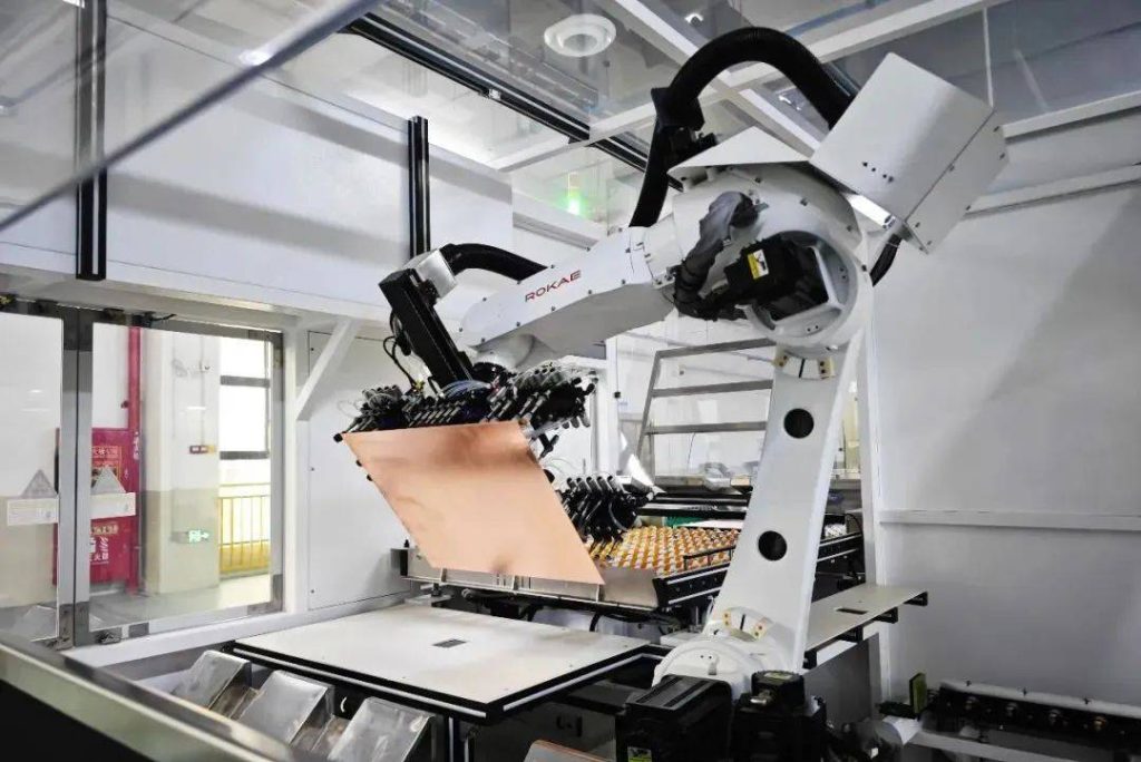
SMT refers to a complete set of standardized production workflows that rely on Printed Circuit Boards (PCBs) as substrates to automate component mounting, soldering and integrated assembly of electronic parts.Circuit board assembly technology serves as the fundamental backbone enabling miniaturization, high performance and mass production of electronic goods within the contemporary electronics manufacturing sector, among which Surface Mounted Technology (abbreviated as SMT) stands as the dominant core manufacturing process across the entire industry.
First invented in the 1960s, this technology has undergone decades of technical iterations, equipment upgrades and process refinements, evolving into a mature, highly efficient and widely adaptable electronic assembly system. Nearly all modern electronic devices rely on SMT for circuit board assembly, ranging from consumer gadgets including smartphones, Bluetooth earbuds and smart wearables to high-end equipment such as industrial controllers, automotive electronics and precision measuring instruments, completely revolutionizing the traditional manufacturing model for electronic products.
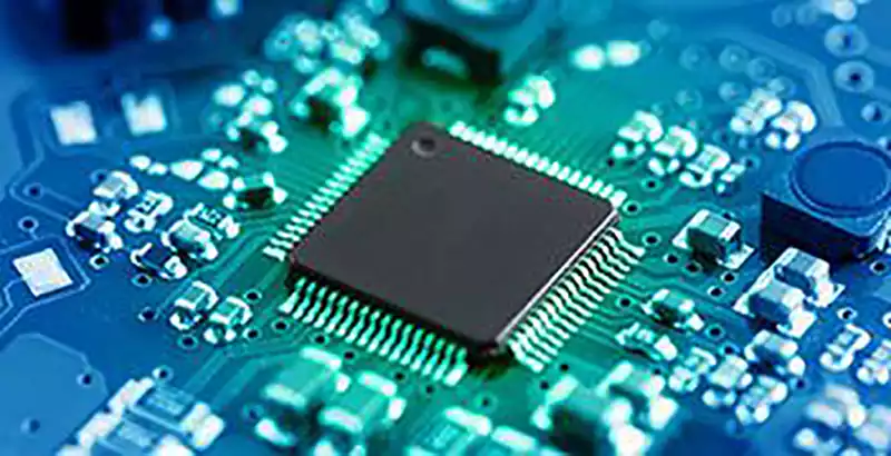
Distinct from legacy circuit board assembly processes, SMT operates on a core design principle that eliminates through-hole pin installation. Instead, surface-mount chip components known as SMC and SMD—parts with no leads or ultra-short terminals—are directly affixed to the exterior surface of PCB substrates before undergoing precision reflow soldering, which establishes both electrical connectivity and physical anchoring between components and circuit boards, making it an advanced assembly solution tailored for modern high-density circuit layouts.
The core merits of SMT can be summarized into four key advantages: superior assembly density, exceptional reliability, enhanced electrical performance and outstanding production efficiency. SMD components occupy merely one-tenth the physical footprint of conventional through-hole parts, deliver robust vibration resistance with minimal solder joint defects, exhibit stable high-frequency characteristics that suppress electromagnetic and radio frequency interference, and lend themselves seamlessly to fully automated manufacturing workflows that cut overall production costs by 30% to 50%.
Finished PCBA, short for Printed Circuit Board Assembly manufactured via SMT, features ultra-high assembly density alongside drastically reduced size and weight; SMD components weigh and measure around one-tenth of classic DIP through-hole plug-in counterparts, shrinking electronic device dimensions by 40% to 60% and slashing total weight by 60% to 80% after SMT implementation.
PCBA products assembled with SMT soldering maintain consistent quality and stable performance, with solid, vibration-resistant solder joints that drastically lower defect rates.
SMT-produced circuit boards deliver steady electrical performance and reduced power consumption thanks to shortened component leads and conductive pathways, which accelerate signal transmission, cut energy usage and mitigate electromagnetic and radio frequency interference while sustaining reliable high-frequency operation.
SMT facilitates full production automation to boost throughput, conserving raw materials, energy, manufacturing equipment, labor resources and production lead times while trimming manufacturing expenses by 30% to 50%.
SMT also carries a handful of inherent limitations: printed numerical markings on miniature components prove difficult to read, complicating maintenance and repair work; component removal and replacement demand specialized professional tools; and mismatched coefficients of thermal expansion (CTE) between mounted components and PCB substrates create structural compatibility risks. These drawbacks have largely ceased to hinder widespread SMT adoption, however, thanks to the emergence of dedicated component rework stations and newly engineered circuit boards built with low thermal expansion coefficients.
Four primary production workflows define standard surface mount assembly operations, starting with the solder paste and reflow soldering process, the most foundational and universally adopted core SMT workflow recognized for streamlined operations, high throughput and precise soldering tolerances. This process requires minimal auxiliary machinery to minimize overall product dimensions, supporting mass manufacturing for nearly all single-layer and mid-sized compact consumer electronics and remaining the preferred assembly solution for consumer electronics manufacturers worldwide.
The second workflow combines component mounting with wave soldering, merging the strengths of surface mount assembly and wave soldering technology to fully utilize dual-sided PCB routing space for further product miniaturization while accommodating low-cost traditional through-hole components. This workflow carries notable drawbacks.
However, including a broader range of required production equipment, tighter process tolerances for wave soldering, elevated rates of soldering defects and incompatibility with ultra-high-density component layouts, restricting its application to low-integration electronic goods prioritizing cost control over compact sizing.
Third is the hybrid assembly process, which unites the benefits of surface mounting and through-hole plug-in assembly to maximize dual-sided PCB space utilization and minimize total circuit board footprint while retaining the cost-effectiveness and superior mechanical durability of through-hole components. Balancing product miniaturization and production expenditures, this highly versatile workflow caters to mass manufacturing of most mid-range electronic devices.
Fourth stands as the dual-sided solder paste reflow soldering process, an exclusive workflow engineered for ultra-compact, high-density electronic products that unlocks the full layout potential of both PCB sides to achieve maximum component integration and minimal assembly area. This process imposes extremely high technical barriers, requiring rigid control over production parameters, complex multi-step workflows and exacting standards for manufacturing equipment precision, factory environmental regulation and process compliance, with primary applications covering mobile communication terminals, miniature smart hardware and premium precision electronic devices that demand dense component packing.
Through Hole Technology, abbreviated as THT, describes the traditional assembly method where electronic components are inserted through pre-drilled PCB holes and permanently secured using molten solder. SMT evolved from legacy THT manufacturing practices yet operates as a fundamentally separate assembly methodology; the core distinction between the two processes lies in their respective installation approaches of surface mounting versus through-hole insertion, with additional disparities spanning substrate design, component specifications, finished assembly geometry, solder joint structure and complete production workflows.
On conventional THT circuit boards, electronic components and their corresponding solder joints sit on opposite sides of the substrate, whereas SMT PCBs place both components and solder contacts on a single board surface. As a result, plated through holes (PTHs) on SMT circuit boards exist solely to connect conductive traces on opposite PCB layers, requiring far fewer holes with significantly smaller diameters and enabling dramatic increases in overall board assembly density.
Four pivotal contrasts separate SMT surface mounting and THT through-hole plug-in assembly, beginning with core production workflows that differentiate surface placement from through-hole penetration. The standard SMT workflow follows three sequential stages: solder paste printing, component mounting and reflow soldering; its transformative innovation eliminates PCB through-hole drilling, unlocking extra routing space for circuit designers and enabling component mounting across both sides of each circuit board.
THT plug-in assembly instead relies on component forming, manual or automated through-hole insertion and wave soldering, with cumbersome multi-step operations constrained by fixed through-hole positioning requirements.
Second, the two technologies diverge drastically in usable space and assembly density, representing SMT’s most pronounced competitive advantage: surface mount components measure and weigh roughly one-tenth of equivalent THT plug-in parts, and hole-free PCB layouts deliver exceptional packing density perfectly suited for compact devices such as smartphones and wearable electronics.
Third, automated mass production efficiency creates another clear divide between the two systems: SMT readily supports fully automated high-speed production lines optimized for large-batch manufacturing with superior cost management capabilities, while THT presents greater obstacles to full automation and frequently creates throughput bottlenecks within modern high-volume production facilities.
Fourth, mechanical anchoring strength highlights THT’s unique competitive edge despite SMT’s density advantages. SMT components feature comparatively weaker physical bonding to PCB surfaces, whereas THT components lock firmly into circuit boards with leads passing fully through drilled holes before soldering, delivering markedly superior structural stability and vibration resistance.
Four major industry driving forces fuel global widespread adoption of SMT technology. First, consumer electronics have continuously trended toward smaller form factors, rendering older through-hole plug-in components incapable of further miniaturization.
Second, modern electronic devices incorporate expanded functional capabilities powered by integrated circuits (ICs) engineered without through-hole pins, especially large-scale and highly integrated IC chips that exclusively rely on surface-mount component packaging.
Third, manufacturers prioritize mass production and full process automation to deliver premium-quality goods at reduced per-unit costs, meeting rising consumer expectations and strengthening market competitiveness against industry rivals.
Fourth, ongoing advancements in electronic hardware, continuous IC development and diversified semiconductor material applications have accelerated electronic technological innovation worldwide, pushing manufacturers to align production processes with global industry standards by adopting mainstream SMT assembly methods.
When measured against traditional THT through-hole plug-in assembly, SMT delivers decisive advantages across component integration density, production throughput, finished product performance and mass production costs, cementing its position as the core enabling technology powering the modern electronics manufacturing industry.
While SMT still presents minor shortcomings including complicated component repair procedures and relatively lower standalone mechanical anchoring strength, continuous process optimization and cutting-edge equipment upgrades consistently expand its viable use cases and amplify its technical benefits. Against the prevailing industry trend toward ever-smaller, higher-performance and intelligent electronic hardware, SMT will maintain its long-term dominance within electronic assembly manufacturing and continue to drive iterative upgrades across the broader global electronics sector