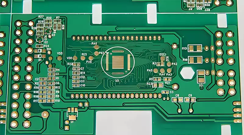
A double sided PCB refers to a PCB board in which both the front and back sides of the substrate are covered with a layer of conductive copper foil, and conductive patterns can be laid out on both sides. Its structure consists of an insulating substrate in the middle and copper foil layers on both sides of the substrate;electrical connections between the two sides of the board are achieved via plated through holes (PTH).
The manufacturing process for plated through-holes involves drilling holes, followed by chemical copper plating and electroplating to form a conductive layer on the hole walls,thereby achieving reliable and stable interlayer interconnection. Compared to single sided pcbs,the most notable feature of double sided pcb board is that circuits can be laid out on both sides of the substrate and connected via through-holes. In terms of manufacturing processes, double sided circuit board involve an additional, crucial step of copper plating (i.e. hole metallisation) compared to single sided pcbs.
Main process flow for double sided PCBs (printed circuit boards):
1.Engineering design and file preparation
Circuit design: Use Electronic Design Automation (EDA) software, such as Altium or KiCad,to draw the circuit schematic.
Layout and Routing: Components are arranged appropriately on both sides of the double sided pcb board, and conductors are connected (located on the Top and Bottom layers respectively).
Generation of Manufacturing Files:
Gerber Files: Graphic information files covering the copper foil, silkscreen and solder mask layers for each layer.
Drilling Files: Used to determine hole positions and diameters, in Excellon format.
IPC Netlist: Used to verify electrical connections.
2.Substrate Preparation Stage
Substrate selection: FR-4 (epoxy glass fibre board) is typically selected, with copper foil applied to both sides.
Cutting: Cut the substrate to the dimensions specified in the design.
3.Inner Layer Pattern Transfer (conducted simultaneously on both sides)
Copper surface cleaning: Remove the oxide layer and contaminants such as oil from the copper surface.
Photoresist Coating: Photoresist (available in both dry and wet film types) is applied evenly to both sides via spraying or rolling.
Exposure Process:
The designed film (photomask) is placed over the copper foil on both sides, then exposed to UV light.In the negative process, the photoresist in the exposed areas hardens.
Development: An alkaline solution is used to dissolve the uncured photoresist, thereby exposing the copper areas to be etched.
4.Etching Stage
Acid Etching: The exposed copper foil is dissolved by spraying with ferric chloride or ammonium copper etching solution.
Stripping: The cured photoresist is removed, leaving the designed copper circuit pattern intact.
5.Laminating and Drilling Process
Oxidation treatment (optional step): To enhance the bond between the copper surface and the resin.
Mechanical drilling operation:
Use a computer numerical control (CNC) drilling machine to drill through-holes and mounting holes.
Key parameter control: Set the drill speed and feed rate appropriately to prevent burrs.
Electrolytic copper plating (PTH) treatment:
Chemical Copper Plating: Depositing a micron-thick conductive layer on the hole walls to metallise the holes.
Copper Plating Thickening: Thickening the copper layer on the hole walls to 20–25 μm to ensure smooth electrical conductivity.
6.Outer Layer Pattern Transfer and Plating Steps
Film lamination, exposure and development: Repeat the procedure in Step 3 to create the outer layer circuit pattern.
Pattern plating process:
Copper plating: Apply a second layer of copper to the circuit traces and via walls to achieve a thickness of 35 μm or more.
Tin plating: Apply a layer of tin to serve as an etching protective layer.
7.Outer Layer Etching and Desoldering Operations
Alkaline Etching: Remove the unprotected copper foil outside the circuit patterns.
Desoldering Treatment: Remove the tin layer to expose the underlying copper circuit patterns.
8.Solder Mask (Green Ink) Treatment
Solder mask ink application: Liquid photosensitive solder mask (commonly green in colour) is applied to the board using screen printing or spraying.
Exposure and development: The areas to be opened (exposing pads and test points) are determined using a stencil.
Curing: The ink is hardened through high-temperature baking.
9.Surface Treatment Processes
Available process types:
Hot Air Solder Leveling (HASL): A layer of tin-lead alloy is plated onto the pads to enhance solderability.
Electroless Nickel Immersion Gold (ENIG): A nickel undercoat is applied first, followed by a layer of gold; this process offers oxidation resistance and is suitable for fine pins.
Organic Solder Preservative (OSP): An organic solder preservative film is applied; this is a lower-cost option but requires soldering to be carried out promptly.
10.Screen Printing Operations
Text Printing: Component part numbers, logos and other information are screen-printed onto the top and bottom layers using white ink.
Curing: The text layer is cured via UV exposure or heat treatment.
11.Forming and Testing Stages
V-Cut or Edge Milling: The panel is cut into individual PCBs.
Electrical Testing (E-Test):
Fly-Probe Testing: Utilises moving probes to check for open circuits or short circuits (suitable for small-batch production).
Testing on a Test Fixture: Uses customised fixtures for batch testing (offering high coverage).
AOI Inspection: Employs automatic optical inspection technology to check for defects in the circuit patterns.
12.Final Inspection and Packaging
Visual inspection/IPC standard sampling: Verification of product dimensions, appearance and functionality.
Vacuum anti-static packaging: Prevents damage and oxidation during transport.
Key Considerations
Alignment accuracy requirements: Double-sided patterns must be strictly aligned, achieved using alignment holes or targets.
Reliability of plated-through holes: The quality of the electroplating process significantly impacts the longevity of interlayer connectivity.
Key Points for Impedance Control: For high-frequency signal lines, precise calculation of trace width and dielectric layer thickness is required.
DFM Optimisation Recommendations: Manufacturing processes must be fully considered during the design phase; for example, sharp-angled traces should be avoided.
Applications of double sided pcb board
Consumer Electronics: Undoubtedly the ‘Giant’ in Terms of Demand
Among the many sectors, consumer electronics leads the way in terms of demand.
Smartphones and Tablets
Although the core motherboards in these devices typically utilise multilayer boards, a vast number of auxiliary modules and interconnect boards—such as camera module boards,fingerprint recognition boards, various sensor boards, keypad boards, battery management boards, headphone jack boards, and certain internal boards within chargers—make extensive use of double sided circuit board.
Computers and Peripherals
Within desktop and laptop computers, double sided PCBs are a common choice for components such as expansion cards, sound cards, certain network interface cards, power supply boards(secondary side), keyboard and mouse boards, monitor driver boards, as well as control boards for printers and scanners.
Home Appliances
Double sided PCBs play a vital role in certain functional modules of television logic boards, as well as in power supply boards, air conditioning control boards, washing
machine control boards, microwave oven control boards, rice cookers, induction hobs,electric fans, and driver boards for smart lighting.
Audio-visual equipment sector
Double sided PCBs are also widely used in audio amplifier boards, Bluetooth speaker mainboards, set-top boxes, certain DVD player boards, and game controller boards.
Smart home devices sector
Double sided PCBs are the ideal choice for numerous products due to their advantages,including various sensors such as temperature and humidity sensors, door and windowmagnetic sensors, and human presence sensors, as well as smart switches, smart sockets,and gateway sub-modules.
Industrial Control and Automation Sector
Control boards for factory automation equipment, sensor interface boards, certain motordriver boards, human-machine interfaces, internal circuit boards for instruments and
meters (such as multimeters, oscilloscope probes and power meters), and PLC I/O modules.
In industrial settings, where reliability and cost are key considerations, double sided PCBs often represent a cost-effective solution that balances performance and cost.
Automotive Electronics Sector
Although the core electronic control units (ECUs) in vehicles typically utilise multilayer boards, the vehicle interior contains a vast array of body control modules. These include headlight driver boards (for lighting control), window control boards, door lock control boards, windscreen wiper control boards, air conditioning control panels, seat adjustment control boards, as well as simple sensor interface boards (such as those found inside tyre pressure monitoring transmitters) and auxiliary boards for infotainment systems. With the ever-increasing level of electronic integration in vehicles, the volume of double sided PCBs used in the automotive electronics sector is immense.
LED Lighting Sector
In the LED lighting sector, whether for bulb lamps, tube lights, panel lights or street lamps, the driver power supply boards almost without exception utilise double sided PCBs.This has become the mainstream and standard configuration in this field, with demand being extremely substantial.
Communications Equipment Sector
In network equipment such as routers, switches and optical network terminals (ONTs),whilst high-performance main chips require multilayer boards to meet their demands,peripheral modules such as power supply modules, interface conversion boards, indicator light boards and fan control boards often utilise double sided pcb board.
Medical Electronics (Medium to Low Complexity Devices)
In blood pressure monitors, blood glucose meters, physiotherapy devices, and certain functional modules of patient monitors—such as sensor boards, display driver boards,keypad boards and power adaptors—double sided PCBs are also a common choice.
Why is the market uptake of double sided PCBs so remarkable?
Exceptional Value for Money
Compared to single sided PCBs, double sided PCBs offer greater functionality, enabling routing on both sides and significantly enhancing routing space and flexibility. When
compared to 4-layer or higher multilayer boards, they offer a significant cost advantage, thanks to their relatively simple manufacturing process, which effectively reduces production costs.
Mature, Stable and Reliable
The manufacturing process for double sided PCBs has undergone long term development and refinement, reaching a high level of maturity. During production, they maintain a high yield rate, and their reliability has been proven over time in the market.They perform excellently in practical applications,providing a solid guarantee for the stable operation of products.
Suitable for a Wide Range of Applications
Among the vast array of electronic products, a large number have moderate functional complexity.Whilst the requirements for signal speed are not extremely high, a certain level of integration is necessary. For such products, double sided PCBs strike an ideal balance between performance and cost, meeting functional requirements without imposing excessive cost pressures.
High Design Flexibility
Through careful layout planning and the judicious use of via technology, double sided PCBs can easily resolve the interconnection challenges of most medium-density circuits. This provides considerable design freedom, enabling designers to implement various circuit functions with greater flexibility.