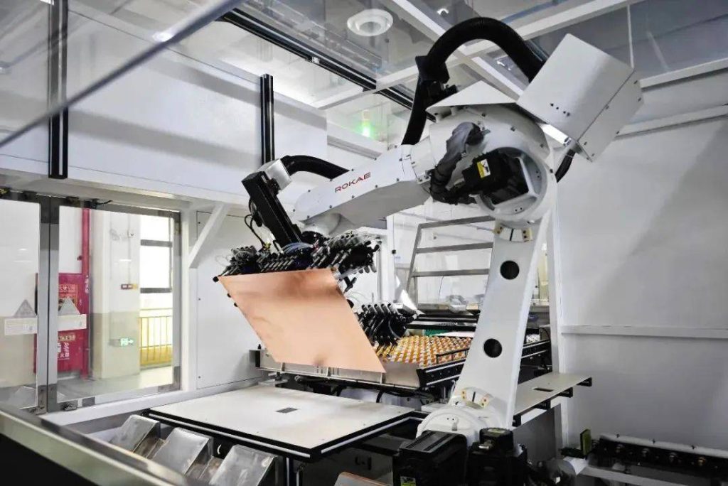
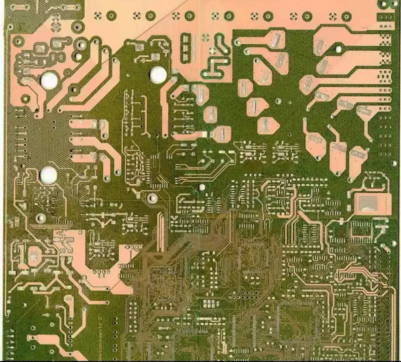
AI pcbs refer to printed circuit boards specifically engineered to support artificial intelligence (AI) server hardware. These boards enable efficient processing of vast datasets, complex computations, and parallel processing by providing electrical connections and signal transmission support for various critical components within AI servers. AI servers are typically deployed for high-performance computing tasks such as deep learning, machine learning, and big data analytics.
Unlike conventional servers, AI servers demand significantly higher hardware performance and computational capabilities, necessitating PCB designs and manufacturing that meet far more stringent technical requirements.
Key Characteristics of AI pcbs
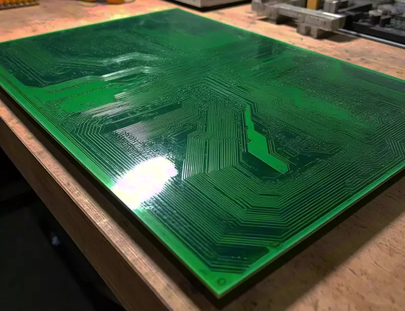
High-Density Interconnect (HDI)
Processing massive datasets requires high-speed, efficient data transfer, leading to the widespread adoption of High-Density Interconnect (HDI) technology in AI pcbs. HDI PCBs feature smaller apertures, finer traces, and higher circuit density, enabling greater component integration and faster signal transmission.
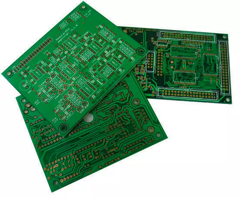
Multi-layer Design
To meet high computational demands, AI servers often incorporate multiple processing units such as CPUs, GPUs, and FPGAs, requiring high-speed electrical connections between them. Multi-layer PCB design facilitates more complex interconnections and circuit layouts within limited space, reducing interference between circuits.
High Current Carrying Capacity
AI servers frequently utilise substantial computational resources, such as multiple GPU cards, necessitating PCBs capable of withstanding significant current loads. PCB materials must exhibit excellent electrical conductivity and thermal resistance. Thick copper PCBs or multi-layer copper foil designs are typically employed to ensure stable power transmission.
High-Frequency Signal Transmission
AI servers frequently handle high-speed data transfer, such as in massively parallel computing where data volumes are immense, necessitating extremely rapid signal transmission. Consequently, PCB design for AI servers must account for high-frequency signal propagation to minimise interference and latency.
Thermal Management
Within AI servers, particularly those incorporating high-performance computing components like GPUs, heat management becomes paramount. The design of AI pcbs typically requires special attention to thermal management, such as employing thermal design techniques alongside effective cooling structures to ensure stable circuit operation.
High Reliability and Durability
AI servers are frequently deployed in environments like data centres, demanding prolonged stable operation. Consequently, the reliability of their PCBs is paramount. Utilising high-quality materials and precise manufacturing processes enhances PCB durability, ensuring stability and safety under extreme operating conditions.
Application Scenarios for AI pcbs
Data Centres
Data centres represent one of the primary application scenarios for AI pcbs. With the rapid advancement of cloud computing and big data, an increasing number of AI servers are deployed within data centres to handle large-scale data processing, storage, and computational tasks.
Cloud Computing Platforms
Cloud computing platforms frequently require extensive parallel computing, where AI pcbs play a crucial role. Whether for natural language processing, image recognition, or intelligent recommendation systems, AI servers require efficient circuit board support to guarantee rapid data transmission and processing capabilities.
Edge Computing Devices
Edge computing represents a distributed computing model, with AI pcbs extensively deployed in smart home systems, autonomous vehicles, industrial automation, and other edge computing devices. These systems necessitate real-time processing of substantial data volumes, demanding circuit board designs that ensure low latency and high performance.
Smart Hardware
AI technology finds extensive application across diverse smart hardware devices, including autonomous vehicles and intelligent medical equipment. These devices demand formidable computational power, rendering AI pcbs indispensable components.
One core task of AI servers is processing vast data volumes and rapidly executing computational tasks through complex algorithms. These tasks typically involve deep learning, massively parallel computing, and real-time inference. Consequently, AI pcbs must meet several critical requirements:
1.High-density interconnections and ultra-high-speed transmission
AI servers must support numerous computational nodes and complex data processing functions. To deliver sufficient computational power, PCB boards require high-density component layouts within constrained spaces. Particularly for accelerators like GPUs, FPGAs, and TPUs used in AI servers, PCB circuit boards must enable ultra-high-speed signal transmission with minimal latency. This necessitates PCB designs employing high-frequency materials, precision routing techniques, and meticulous signal integrity management.
2.Exceptional thermal management
AI servers process vast quantities of data, with computational tasks typically generating significant heat. Consequently, thermal management must be integral to AI server PCB design. The PCB’s thermal performance directly impacts system stability and reliability. To address this, many AI servers employ multi-layer PCB substrate structures, employing optimised layouts, dedicated heat channels, and enhanced thermal materials to ensure effective heat dissipation and prevent hardware damage from overheating.
3.High Reliability and Stability
AI servers typically operate continuously around the clock, necessitating PCB boards with exceptional reliability and stability. Even minor electrical faults or signal interference can degrade system performance or cause complete system failure. To guarantee high stability, AI server PCB design requires high-quality raw materials, meticulous electrical layout, and precise soldering techniques to eliminate any potential stability risks.
4.Miniaturisation and Multifunctional Integration
As AI applications expand into edge computing and mobile devices, AI server PCB design must not only meet data centre performance demands but also achieve a degree of miniaturisation to accommodate diverse deployment scenarios. This requires designers to minimise PCB dimensions while maintaining performance, integrating multiple functions onto a single circuit board.
With the continuous advancement of AI technology, the demand for AI servers continues to grow, driving innovation in PCB design and manufacturing. Below are some cutting-edge technologies currently applied in AI server PCB design:
1.HDI (High-Density Interconnect) Technology
HDI PCB technology fulfils AI servers’ requirements for high density and high speed by enabling more complex circuit connections within smaller spaces. HDI boards typically employ smaller apertures and finer line widths, facilitating greater signal transmission within more limited areas and thereby enhancing overall computational capability.
2.Flexible Printed Circuits (FPC)
With increasing demands for flexibility and slimline designs in AI equipment, flexible printed circuits (FPC) are gaining traction within AI server applications. Flexible PCBs not only offer greater design freedom but also enable circuit boards to adapt to diverse server form factors. Their implementation enhances system integration and thermal management capabilities while reducing board footprint.
3.High-Speed Signal Transmission Materials
Within AI servers, communication between processors and accelerators necessitates ultra-high-speed signal transmission. Consequently, AI pcbs typically employ high-frequency, high-speed materials such as PTFE (polytetrafluoroethylene) or ceramic substrates to ensure signal transmission stability and accuracy. Utilising these high-performance materials effectively reduces signal attenuation and interference, thereby enhancing computational performance.
4.Multilayer PCB Design
AI servers frequently employ multi-layer PCB designs, distributing circuits across distinct layers. By optimising multi-layer layouts, designers can segregate power planes, signal planes, and ground planes, thereby reducing mutual interference and enhancing signal integrity. Concurrently, multi-layer designs effectively control signal delay and noise, improving transmission efficiency.
AI pcbs constitute one of the core hardware components underpinning modern artificial intelligence technology, demanding exceptionally stringent design and manufacturing requirements. With the rapid advancement of AI technology, the hardware architecture of AI servers continues to innovate, driving progress in the field of PCB design.
Looking ahead, as AI applications expand from data centres to edge computing devices, AI pcbs will face heightened challenges and broader application demands. Designers must balance high performance with miniaturisation, multifunctional integration, and cost-effectiveness, propelling technological advancement and providing a robust hardware foundation for innovation in the AI domain.