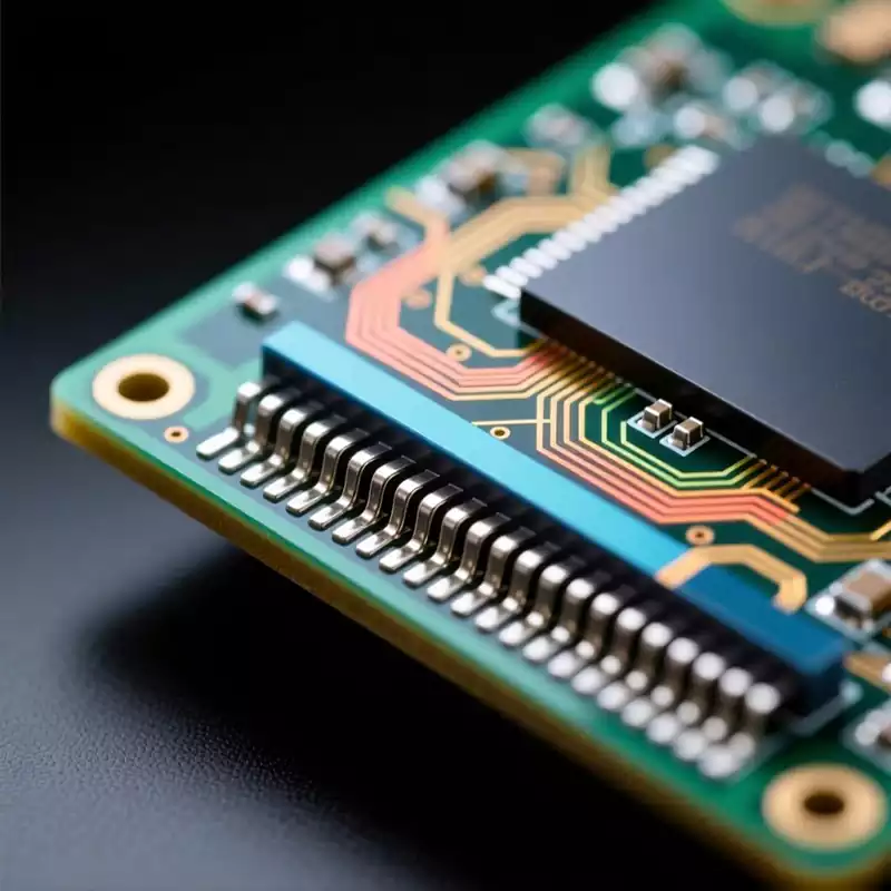
Electroless nickel immersion gold (ENIG) and electroplated nickel-gold plating represent the two predominant surface treatment solutions for LTCC ceramic substrates. Whilst both employ a core principle of ‘nickel underlay with gold overlay for protection’, they exhibit significant differences in process fundamentals, performance characteristics, and suitable applications.
Process Principles
The core objective of both ENIG and electroplated nickel-gold is to form a composite structure of ‘nickel layer + gold layer’ on the surface of LTCC ceramic substrates. However, the fundamental differences in their implementation methods determine their distinct performance characteristics and applicable scenarios.
Electroless nickel-gold (ENIG) employs a chemical deposition reaction to achieve nickel-gold coverage. Requiring no external power source, it relies solely on reducing agents within the electroless plating solution to initiate redox reactions, progressively depositing nickel and gold ions onto the ceramic substrate surface. The entire process relies on self-catalysed chemical reactions without electrical current. Coating thickness uniformity is controlled by the plating solution concentration, reaction temperature, and processing time. It enables uniform deposition across complex substrate structures and is a purely chemical deposition process.
Process flow for gold deposition
Pre-treatment: Surface activation
The LTCC ceramic substrate undergoes degreasing and micro-etching to thoroughly remove surface contaminants, impurities, and natural oxide layers. This simultaneously creates a uniform micro-rough surface structure, providing a stable foundation for subsequent nickel deposition and ensuring robust adhesion between the coating and substrate.
Electroless nickel plating: Formation of nickel-phosphorus alloy layer
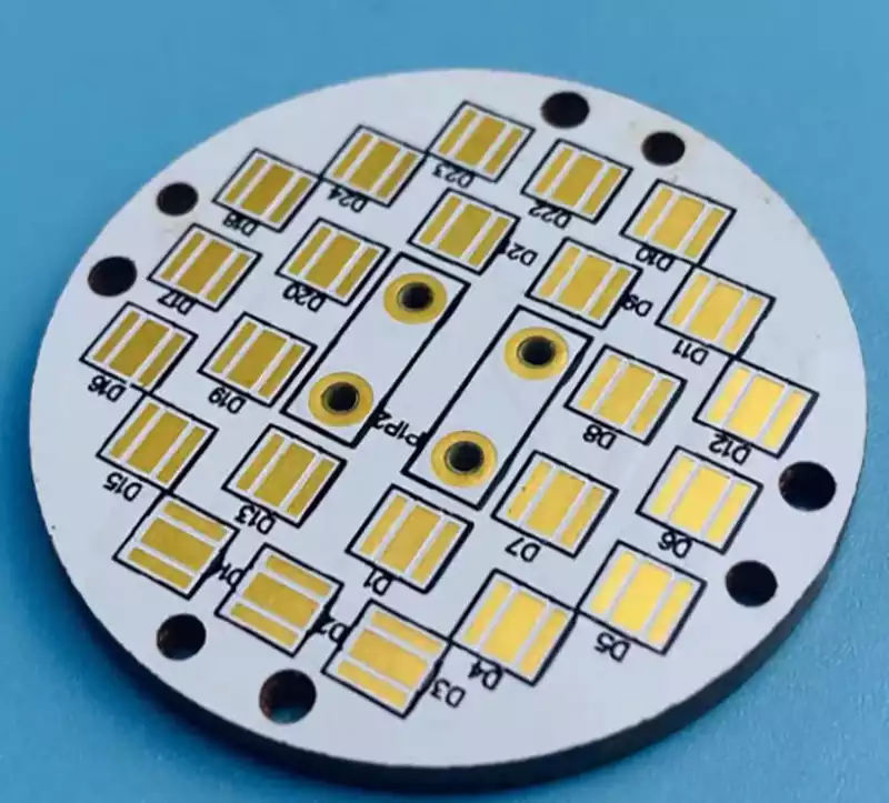
The pre-treated substrate is immersed in an electroless nickel plating solution. Under the action of a catalyst, the hypophosphite in the plating solution undergoes a redox reaction, reducing nickel ions to metallic nickel which deposits onto the substrate surface. This ultimately forms a nickel layer with a thickness of 2–8 μm. This process involves the generation of a small amount of phosphorus (phosphorus content 7%-11%), resulting in the formation of a nickel-phosphorus alloy layer rather than a pure nickel layer.
Electroless Gold Plating: Depositing a Thin Gold Protective Layer
Following the formation of the nickel-phosphorus alloy layer, a thin gold layer with a thickness of 0.05-0.3μm is deposited onto its surface via a displacement or reduction reaction. The primary function of the gold layer is to protect the nickel layer from oxidation while enhancing the substrate’s solder compatibility.
Key characteristics of the entire process: It relies entirely on self-catalysed chemical reactions without requiring an external electrical current. Coating thickness uniformity is controlled by the plating solution concentration, reaction temperature, and processing time. It enables uniform deposition across the entire surface of substrates with complex structures and is a purely chemical deposition process.
Electroplating nickel-gold, conversely, achieves coating deposition through electrolytic reactions. This requires an external direct current power supply, with the LTCC ceramic substrate serving as the cathode and nickel and gold plates functioning as anodes, immersed in corresponding electroplating solutions. Upon energisation, under the influence of the electric field, nickel ions/gold ions dissolve from the anodes into the plating solution. These ions then migrate towards the cathode substrate surface, where they are reduced and deposited to form the metallic coating. The process sequence similarly comprises three major stages: pre-treatment, nickel plating, and gold plating.
However, the technical rationale for each stage differs from that of direct gold plating:
Pre-treatment: Enhancing Conductive Activation
The fundamental process comprises degreasing and micro-etching (identical to gold plating). The core distinction lies in the additional requirement for ‘conductivity treatment’—physically or chemically forming a conductive film on the insulating ceramic substrate surface. This ensures the substrate can function as a cathode in subsequent electrolytic reactions, preventing coating deposition failure due to lack of conductivity.
Electroplating Nickel: Precise Control of Pure Nickel Layer Thickness
Establishing the Electrolytic System: Using an LTCC ceramic substrate as the cathode and a pure nickel plate as the anode, both are immersed in the nickel plating solution. Upon application of an external DC power supply, the electric field causes nickel ions from the anode to dissolve into the plating solution. These ions then migrate directionally to the cathode substrate surface, where they undergo reduction and deposition, forming a pure nickel layer. By adjusting the current density, the nickel layer thickness can be precisely controlled (typically 3-15μm). The resulting coating comprises high-purity metallic nickel, free from phosphorus elements.
Electroplating Gold: Flexible Adjustment of Gold Layer Specifications
Continuing the electrolytic system logic: Replace the anode with a pure gold plate and immerse it in the gold plating solution. Similarly, under the driving force of the electric field, gold ions selectively deposit onto the nickel layer surface, forming a gold layer. Depending on application requirements, gold layer thickness can be flexibly selected: thin gold (0.1-0.5μm) for standard protection and soldering, thick gold (1-5μm) for bonding or high-protection scenarios.
Performance Differences
The differing process principles directly result in significant variations between gold plating and electroplated nickel-gold in key metrics such as coating structure, soldering performance, reliability, and cost. These differences form the core basis for selection.
In terms of coating uniformity and coverage capability, electroless gold plating demonstrates superior performance. As it does not require an electric current, the process remains unaffected by substrate geometry or circuit density. It can form a uniform coating on complex structures such as fine traces, blind vias, and grooves within LTCC ceramic substrates, with minimal thickness variation. Electroplated nickel-gold, however, is susceptible to electric field distribution. This often results in excessively thick plating at substrate edges and circuit corners, while thin plating or even plating gaps may occur at blind via bottoms and inter-track spaces. It is particularly unsuitable for high-density, fine-line LTCC ceramic substrates. For instance, on LTCC ceramic substrates with line widths/spacings below 50μm, the plating uniformity deviation of electroless gold plating can be controlled within ±10%, whereas that of electrolytic nickel-gold plating may exceed ±20%.
Regarding soldering reliability, both methods have distinct advantages and disadvantages. The nickel-phosphorus alloy layer of electroless gold exhibits excellent wettability with solder. Thin gold layers dissolve rapidly into the solder, forming stable intermetallic compounds (IMCs) that yield high solder joint strength. However, the phosphorus in the nickel-phosphorus alloy may form brittle nickel-phosphorus compounds during high-temperature soldering. Excessively high temperatures or prolonged soldering times can lead to solder joint cracking. Electroplated nickel-gold’s high-purity nickel layer exhibits superior compatibility with solder, yielding more stable intermetallic compounds and enhanced soldering reliability, while withstanding multiple reflow cycles. However, if the thick gold layer fails to dissolve completely, it may induce gold embrittlement, compromising joint strength. Consequently, thin gold plating is generally recommended for soldering applications in electroplated nickel-gold processes.
In terms of corrosion resistance and service life, electroplated nickel-gold offers superior advantages. The thin gold layer (0.05–0.3μm) in immersion gold plating primarily serves a protective function. Under prolonged use or exposure to harsh environments, the gold layer is prone to wear or corrosion, which in turn compromises the underlying nickel layer. Electroplated nickel-gold, however, permits thicker gold plating, offering superior protective capabilities. Moreover, the oxidation resistance of high-purity nickel layers surpasses that of nickel-phosphorus alloy layers, making it suitable for applications demanding extended service life. For instance, LTCC ceramic substrates used in outdoor environments or high-temperature, high-humidity conditions exhibit a service life 2-3 times longer with thick electroplated gold compared to immersion gold.
Regarding cost, electroless gold plating offers better value for money. The gold layer thickness in electroless gold plating is only 0.05-0.3μm, resulting in significantly lower gold consumption compared to electroplated nickel-gold (especially thick gold solutions). Additionally, the per-use cost of the chemical plating solution is lower. In contrast, electroplated nickel-gold deposits feature thicker layers and higher gold consumption. Combined with the higher capital investment and energy costs of electroplating equipment, the unit area processing cost is typically 1.5-3 times that of electroless gold plating. For mass-produced conventional LTCC ceramic substrates, the cost advantage of electroless gold plating is particularly pronounced. However, in specialised scenarios requiring localised thick gold layers and high reliability, the cost premium of electroplated nickel-gold plating can be offset by its performance benefits.
Furthermore, regarding compatibility with subsequent processing, electroless gold plating is more suitable for soldering applications, while electroplated nickel-gold plating is better suited for bonding applications. The thin gold layer of electroless gold plating rapidly fuses with solder, eliminating the risk of gold embrittlement from residual gold layers. Conversely, the thick gold layer of electroplated nickel-gold plating meets the requirements for gold wire bonding and gold ribbon bonding, offering high bonding strength and excellent stability. This makes it a common solution for RF and microwave LTCC ceramic substrates.
Ceramic Substrate Scenario-Based Selection Strategy
High-Frequency Communication Modules (5G/Millimetre Wave Applications)
Significant Advantages of Immersion Gold Process
Superior Skin Depth Stability: Gold layer thickness variation controlled within ±8%. At 77GHz, this significantly enhances signal integrity by up to 40%.
Outstanding Low Oxidation Characteristics: After 24 hours of environmental exposure, contact resistance increases by only 2%, compared to an 8% rise with gold plating.
Typical Applications: Frequently used in active antenna unit (AAU) arrays for base stations and satellite transmit/receive (T/R) components.
High Power Density Packaging Applications (SiC/GaN Device-Related)
Significant Advantages of Immersion Gold Plating
Excellent thermal expansion matching: Nickel’s coefficient of thermal expansion (CTE) of 13 ppm/°C aligns well with ceramic substrates’ CTE of 6–8 ppm/°C.
Strong ion migration resistance: No failures observed after exceeding 5,000 hours of ageing tests at 85°C and 85% relative humidity.
Typical Applications: Widely employed in electric vehicle motor controllers and photovoltaic inverters.
Miniaturised 3D IC Packaging Applications
Significant Advantages of Immersion Gold Plating
Superior Surface Co-planarity: Pad height variation is less than ±3μm, supporting micro-bump pitches as fine as 10μm.
Thin Interface Transition Layer: Its interface transition layer measures merely 30nm thick, whereas electroplated gold exhibits a transition layer exceeding 80nm.
Within LTCC ceramic substrate applications, the gold immersion process has become the preferred choice for high-reliability electronic systems due to its excellent compatibility with non-conductive substrates, exceptionally low surface roughness (Ra value below 0.06μm), and outstanding thermomechanical reliability. It holds a dominant position in 5G millimetre-wave technology and third-generation semiconductor fields. Conversely, electroplated gold retains irreplaceable advantages in high-wear-resistance insertion/removal applications, such as military connectors. Looking ahead, with the continuous advancement of low-temperature co-fired ceramic (LTCC) technology and heterogeneous integration techniques, the immersion gold process will persistently evolve towards nanometre-level precision and ultra-thin profiles. This progression will facilitate major technological breakthroughs in 6G communications and quantum devices.