The routing design of ceramic PCBs constitutes one of the core elements determining their electrical performance, thermal dissipation capabilities, and long-term reliability. In applications demanding high power density, high frequencies, and high integration, the limitations of traditional FR-4 PCBs in thermal conductivity, dimensional stability, and long-term environmental adaptability are becoming increasingly apparent. They are no longer sufficient to meet the requirements of power electronics, RF modules, and demanding industrial environments. Owing to their high thermal conductivity, structural stability, and superior electrical consistency, ceramic PCBs are progressively becoming a vital foundational platform for high-performance electronic systems.
However, the material advantages of ceramic PCBs do not automatically translate into enhanced system performance. Only through routing strategies tailored to their material and structural characteristics can their comprehensive value in electrical performance, thermal management, and reliability be fully realised. Scientific routing design not only influences signal and current transmission quality but also directly determines heat dissipation pathways, manufacturing feasibility, and product stability under long-term operational conditions.
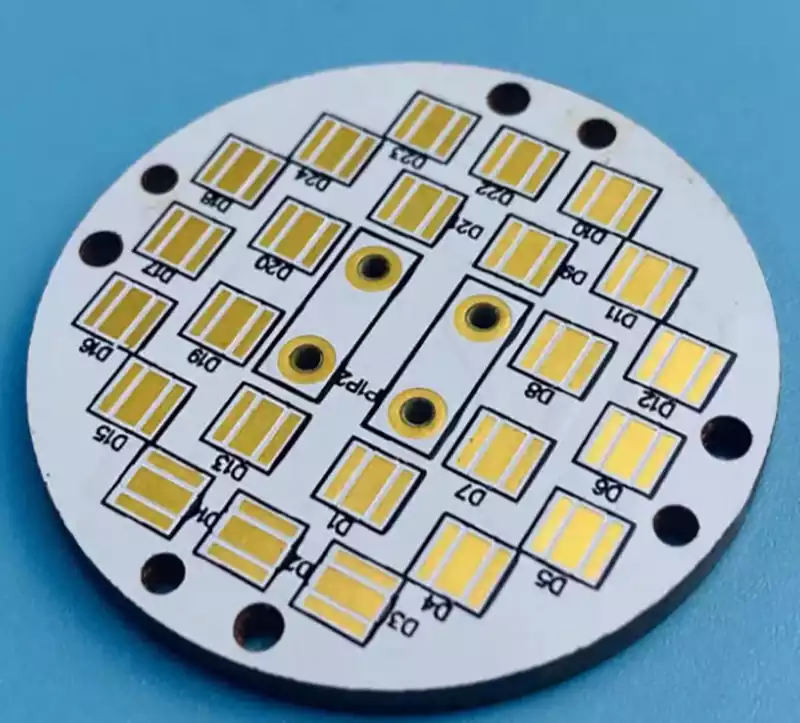
In typical ceramic PCB applications, distinct functional loops exhibit significant variations in current ratings, thermal loads, and electromagnetic characteristics. Power loops typically carry high currents and transient energy, serving as primary heat sources while also posing potential electromagnetic interference risks; Drive and control circuits are usually tightly coupled with power devices, demanding high timing stability and noise immunity; detection or communication signal circuits primarily handle small signals, being particularly sensitive to signal integrity and environmental stability. If these circuits are physically interleaved in layout, even with established electrical connections, systemic hazards such as thermal coupling, crosstalk, and ground potential fluctuations become difficult to avoid.
Therefore, a clear functional zoning strategy should be incorporated into the routing of ceramic PCBs from the layout stage. Design focus should not solely revolve around component dimensions but rather be based on loop characteristics for regional division. Power loops should be concentrated in locations offering optimal thermal dissipation and ease of heat transfer. Their routing objectives are to achieve the shortest path, minimal loop area, and clear current flow direction, while reserving sufficient copper area to avoid later constraints such as reduced line widths or fragmented copper surfaces due to space limitations. Drive and control loops should be physically proximate to their corresponding power components to minimise control paths, whilst maintaining reasonable spacing from primary power traces to prevent passive crossing of high-current zones that could introduce noise. Detection and communication signal loops should be prioritised for placement away from high-power areas or isolated using natural copper plane boundaries to achieve a relatively stable and controllable electromagnetic and thermal environment.
Under this top-down functional zoning and prioritisation scheme, routing ceases to be mere spatial filling and becomes an active design process centred on system objectives. Power loops receive priority allocation of space and copper resources; control loops ensure path integrity first; signal loops guarantee environmental purity first. This approach prevents compromises later in the process during the routing stage.
At the detailed routing level, ceramic PCB routing must be co-designed with thermal paths. For high-heat-generating components, copper layer continuity is paramount. Heat from power devices first enters the copper layer in direct contact. If narrow traces, frequent necks, or fragmented copper surfaces are employed beneath or near the device, heat diffusion is impeded during its initial phase, readily causing localised thermal accumulation. Such issues stem not from the ceramic material itself, but from artificially introduced thermal resistance within the routing structure.
Consequently, high-power circuits within ceramic PCBs should prioritise large, continuous copper areas over relying on multiple parallel fine traces to meet current-carrying requirements. Continuous copper zones not only substantially reduce resistance and parasitic inductance but also facilitate rapid heat diffusion in the planar direction, achieving effective thermal uniformity. When heat is distributed across a larger copper area, the heat flux density per unit area significantly decreases, creating more favourable conditions for subsequent vertical heat transfer.
In this process, the ceramic substrate’s high thermal conductivity plays a pivotal role. The low thermal resistance copper-ceramic interface formed via DBC or AMB processes enables heat, already evenly distributed in the planar direction, to be efficiently conducted vertically into the ceramic substrate and further transmitted to its rear surface. This establishes a synergistic thermal conduction mechanism where ‘the copper layer handles lateral heat distribution while the ceramic substrate manages vertical heat extraction,’ transforming the wiring itself into an integral component of the thermal management structure.
Concurrently, the routing of power traces should align as closely as possible with primary thermal diffusion pathways, avoiding unnecessary openings, isolation slots, or constricted connection points along critical heat transfer routes. This approach minimises thermal flow detours, enhances thermal conduction efficiency, and renders heat distribution more predictable.
Hierarchically, ceramic PCBs are ill-suited to excessive reliance on multi-layer stack-ups and dense via patterns. Compared to FR-4 PCBs, ceramic substrates present greater challenges in drilling and metallisation; increasing via counts significantly elevates manufacturing costs and reduces yield rates. Electrically, vias introduce additional parasitic parameters and elongate current paths, compromising impedance control in high-current or high-speed switching scenarios. From a thermal management perspective, frequent layer-to-layer jumps disrupt copper continuity, creating thermal diffusion bottlenecks. Regarding reliability, via regions often concentrate thermal and mechanical stresses.
Consequently, ceramic PCB routing should prioritise single-layer or minimal-layer structures, completing critical current paths within a single layer wherever possible to minimise unnecessary layer transitions. Where vias are unavoidable, adhere to the principle of “fewer but better”, strictly limiting their quantity while rationally designing aperture size, wall metal thickness, and positioning to avoid interference with primary current and thermal pathways.
Overall, effective ceramic PCB routing should centre on the core principles of “clear functional zoning, continuous copper planes, direct paths, and simplified structure”. By integrating electrical connectivity, thermal diffusion, and structural integrity into routing decisions, designers can fully leverage the material and structural advantages of ceramic PCBs in high-power, high-reliability applications without relying on additional complex structures. This concept of electro-thermal co-design represents the fundamental characteristic that distinguishes ceramic PCBs from traditional organic PCBs.