As optical modules are employed for high-speed data transmission and optoelectronic conversion, the manufacturing quality of their PCBs directly impacts the performance, stability, and reliability of the optical modules.
Key requirements in optical module PCB manufacturing:
1.High-precision manufacturing
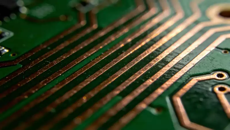
Optical module PCB design demands exceptional accuracy to ensure stable and complete signal transmission. During high-speed data transfer, even minute errors may cause signal attenuation, distortion, or interference. Consequently, the manufacturing process must meet the following precision requirements:
Fine line width and spacing: As signal frequencies increase, optical module PCBs require exceptionally fine line widths and spacing. Typically, tolerances for line width and spacing are specified at the micrometre level.
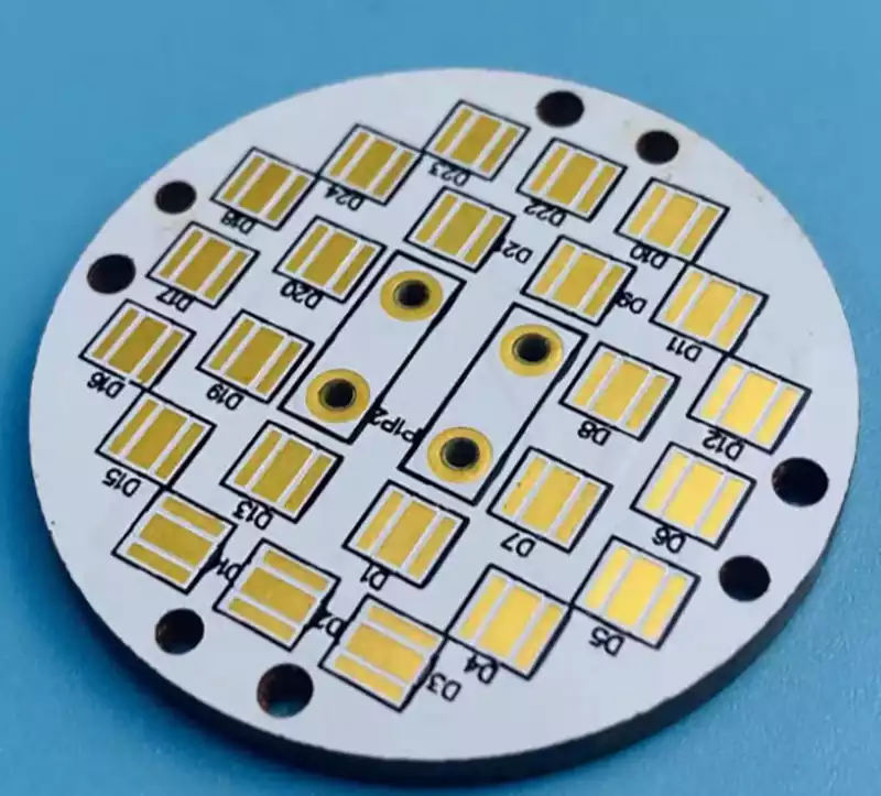
Small aperture and high-density routing: High-density interconnect (HDI) technology is employed to achieve smaller apertures and greater signal pathways. Precision drilling and micro-machining techniques ensure seamless implementation of high-density routing.
2.High-Frequency Materials and Precise Control
Optical module PCBs necessitate high-frequency materials to guarantee stable signal transmission and low loss. Materials such as PTFE (polytetrafluoroethylene) and ceramic substrates offer low dielectric constants and low loss, making them suitable for high-speed signal transmission. Manufacturing requirements include:
Precise Material Cutting and Processing: When utilising these high-frequency materials, exacting cutting and handling are essential to prevent degradation or inconsistencies in material properties.
High-Precision Laminating Technology: The laminating process necessitates high-quality materials to ensure electrical performance meets standards. Temperature and pressure during lamination must be precisely controlled to avoid circuit performance degradation due to unevenness.
3.Thermal Management Control
Given the substantial heat generated during optical module operation, PCB manufacturing must address thermal management. Particularly in high-density designs and high-power optical modules, the manufacturing process must guarantee effective heat dissipation. Requirements include:
Optimal copper thickness design: Copper thickness directly impacts PCB thermal conductivity. Thicker copper foil enhances thermal conductivity, facilitating faster heat dissipation.
Heat dissipation channels and thermal diffusion design: During PCB design, strategically arrange heat dissipation pathways and thermal diffusion routes to ensure effective heat dispersion through the board, preventing overheating that could compromise module performance.
4.Precise Multilayer Laminating Technology
PCBs for optical modules often employ multilayer designs to achieve high-density signal interconnections. Multilayer PCB design imposes stringent requirements for the layered organisation of power, ground, and signal planes. Manufacturing requirements include:
Laminating Technology: During multilayer PCB production, precise control of the lamination process between each layer is essential to ensure accurate alignment, preventing misalignment or soldering defects between layers.
Interlayer Electrical Connection Quality: Ensuring stable electrical connections between layers avoids signal loss or interference caused by poor interlayer connections.
5.Signal Integrity Management
Signal integrity is paramount for optical module PCBs, as it directly impacts data transmission quality. During optical module PCB manufacturing, signal transmission pathways must be safeguarded against loss, attenuation, or interference:
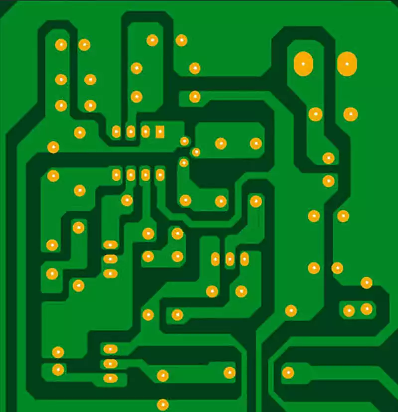
Precise Signal Routing: Signal traces must be as straight as possible, minimising excessive turns to reduce reflection and attenuation. Manufacturing requires precise control over trace width, spacing, and impedance matching.
Impedance control: Signal transmission in optical modules typically requires stringent impedance control. Manufacturing must ensure consistent impedance for differential signal lines to prevent signal distortion and interference.
6.Electromagnetic Interference (EMI) Control
High-speed signal transmission is susceptible to electromagnetic interference (EMI), necessitating effective EMI control measures during optical module PCB manufacturing:
Shielding Design: Employ metal shielding enclosures or electromagnetic shielding materials to reduce electromagnetic radiation. Shielding layer design must be precise and ensure effective connection to the ground plane.
Ground Plane Design: A well-planned ground plane layout minimises electromagnetic interference. Manufacturing must guarantee a uniform, defect-free ground plane to prevent ground loops.
7.Power Management and Noise Control
Optical modules require stable power supply during operation, demanding stringent power plane design during manufacturing:
Power Plane Design: Power planes and ground planes must be separated to ensure power stability and minimise interference. Power planes should employ multiple layers of copper foil to provide adequate current-carrying capacity.
Noise Suppression: Reduce the impact of power supply noise on signal transmission by incorporating decoupling capacitors and filter circuits. During manufacturing, precise positioning and connection quality of decoupling capacitors and filter circuits must be guaranteed.
8.Reliability and Durability Requirements
Optical modules are typically deployed in demanding environments such as data centres and communication networks, making PCB reliability and durability paramount:
High-Quality Material Selection: Employ premium PCB materials to ensure stable electrical performance, resistance to high temperatures and humid heat, and prevent degradation or failure during prolonged operation.
Vibration-Resistant Design: As optical modules often operate in dynamic environments, PCB manufacturing must incorporate vibration and shock resistance to ensure stable circuit operation under severe environmental fluctuations.
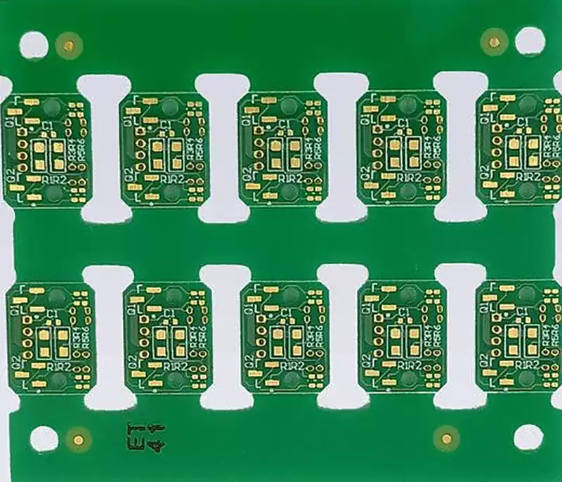
9.Rigorous Manufacturing Processes and Quality Control
Optical module PCB production demands stringent quality control to ensure compliance at every stage, preventing manufacturing defects from compromising module performance. Common quality control steps include:
Lamination Quality Inspection: During lamination, precise alignment of each layer is essential to prevent bubbles or unevenness.
Automated Inspection and Testing: Post-manufacturing, automated equipment verifies that each board meets performance requirements, particularly regarding signal integrity, impedance matching, and power management.
FAQ
1.What tolerance level is required for trace width and spacing on optical module PCBs?
Answer: Typically within the micrometre range to accommodate high-speed signal transmission and prevent signal attenuation or distortion.
2.Why is impedance control critical for optical module PCBs?
Answer: Strict impedance control ensures consistent differential signal line impedance, preventing signal distortion and interference to safeguard data transmission quality.
3.How do technological advancements in optical modules impact PCB manufacturing?
Answer: These advancements demand higher precision in PCB manufacturing, superior material properties, and more complex processes. Design optimisation, process refinement, and enhanced quality control procedures are required to meet evolving requirements.
4.What high-frequency materials are commonly used for optical module PCBs?
Answer: Materials such as PTFE (polytetrafluoroethylene) and ceramic substrates are frequently employed. These offer low dielectric constants and minimal loss, making them suitable for high-speed signal transmission.
The manufacture of optical module PCBs constitutes a high-precision, technically demanding task encompassing signal transmission, thermal management, and power supply design. As optical communication technology advances, increasingly stringent requirements for optical modules elevate the technical complexity of PCB manufacturing. Only through precise design, meticulous manufacturing processes, and rigorous quality control can the stability and reliability of optical module PCBs be assured during high-speed, high-frequency, and prolonged operation.