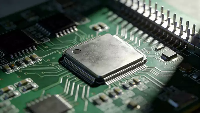
Optical Module PCB refers to the printed circuit board (PCB) used within optical modules. It serves to mount components such as optoelectronic chips, driver circuits, and control chips, enabling high-speed signal transmission, electro-optical/optical-electrical conversion, and thermal management. Optical modules are critical components in modern optical communication systems, typically employed to convert electrical signals into optical signals (via lasers) or to convert optical signals back into electrical signals (via photodetectors), thereby facilitating high-speed data transmission. The optical module PCB serves as the physical carrier for the internal circuits and components within the optical module.
Primary Functions of the Optical Module PCB
Signal Transmission and Processing: The core task of an optical module is to convert between electrical and optical signals. The PCB circuit board houses the module’s internal circuitry, including circuits for driving the laser, detectors for receiving photoelectric signals, and circuits for signal processing and modulation.
Optoelectronic Interface: The PCB board connects critical optoelectronic components within the module, such as lasers and photodetectors. These components require efficient circuitry to interface with other electronic elements, ensuring precise signal conversion.
Thermal Management: Optical modules generate heat during operation, particularly high-performance variants. The PCB circuit board necessitates well-designed thermal pathways to facilitate effective heat dissipation, preventing overheating that could compromise module stability.
Power Management: Optical modules require stable power supply for operation. The PCB must incorporate power distribution circuits to deliver consistent voltage and current, thereby guaranteeing normal module function.
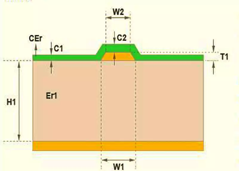
Common PCB materials for optical modules fall into two primary categories: traditional FR4 substrates and specialised high-frequency/high-speed materials. Below are several materials frequently used in optical module PCBs:
1.FR4 (Standard Glass-Fibre Board)
FR4 is one of the most prevalent PCB substrate materials, extensively used in circuit boards for general electronic products. However, despite its cost advantages, it is unsuitable for handling extremely high frequencies or high-speed signals. As optical modules typically involve high-speed signal processing, particularly at 100Gbps, 400Gbps, or even higher bandwidths, FR4 is generally not appropriate for all types of optical module PCB designs.
Characteristics: Relatively low cost, easy to process, suitable for low-frequency signals and general applications.
Limitations: FR4 material exhibits limited high-frequency performance with significant signal attenuation. This may cause signal integrity issues, particularly in high-speed data transmission and high-density integrated optical modules.
2.PTFE (Polytetrafluoroethylene)
PTFE (such as Rogers 4003C, Rogers 5880, etc.) is a high-frequency PCB material commonly employed in applications demanding high speed and performance, such as optical module PCBs. PTFE exhibits excellent electrical properties, effectively reducing signal loss and enhancing transmission stability, making it particularly suitable for high-speed signal transmission and radio frequency (RF) applications.
Characteristics: Features an exceptionally low dielectric constant and dielectric loss factor, making it suitable for high-speed, high-frequency applications.
Advantages: Extremely low signal attenuation, outstanding high-frequency performance, and suitability for high-speed signal transmission.
Application Scenarios: Suitable for high-bandwidth optical modules, such as 100Gbps and higher-speed optical module designs.
3.Ceramic Substrates
Ceramic substrates, such as Al₂O₃ (aluminium oxide) and AlN (aluminium nitride), represent high-performance PCB materials with outstanding thermal conductivity and electrical properties. They are particularly suited for optical modules requiring advanced thermal management and high-frequency performance. Their superior thermal conductivity effectively aids heat dissipation, preventing performance degradation due to overheating.
Characteristics: High thermal conductivity, high-temperature resistance, favourable electrical properties.
Advantages: Ceramic materials deliver outstanding thermal management capabilities, making them highly suitable for high-power and high-speed signal applications.
Application Scenarios: Widely employed in high-frequency, high-power optical module designs, particularly in applications demanding robust thermal management such as data centres and high-speed communication equipment.
4.Polyimide
Polyimide (PI) is a flexible material that can also be employed in optical module PCB design. Its advantages include providing greater flexibility, making it suitable for optical module designs requiring a degree of bending or adaptation to varied spatial constraints. Polyimide further exhibits excellent high-temperature resistance and electrical properties.
Characteristics: High temperature resistance, flexible design, suitable for miniaturised and high-density integration designs.
Advantages: Suitable for optical module designs requiring bending or integration within limited spaces.
Application Scenarios: Suitable for optical module applications demanding miniaturisation and constrained space, such as those in mobile communications and embedded systems.
5.Low Loss Substrates
Optical module PCBs frequently utilise low-loss substrate materials from brands such as Isola, Taconic, and Rogers. These possess low dielectric loss factors, effectively reducing signal attenuation during transmission and ensuring high-frequency signal stability.
Characteristics: Low dielectric loss, suitable for high-speed signal transmission.
Advantages: Reduces signal attenuation, enhancing signal stability and transmission quality.
Application Scenarios: Suitable for high-speed, long-distance data transmission, such as in fibre optic communications and data centre optical modules.
6.Silicon-based Substrates
With technological advancements, silicon-based materials (e.g., silicon photonics) are being incorporated into certain optical module designs. Silicon substrates enable the integration of more optical components and electronic circuits, facilitating optoelectronic co-design. They effectively combine optical devices with circuitry, reducing module size while enhancing performance.
Characteristics: High integration level, suitable for optoelectronic integration.
Advantages: Capable of tightly integrating optoelectronic components with electronic circuits, suitable for miniaturised optical modules.
Application Scenarios: Suitable for optical module designs requiring high-density integration and silicon photonics.
Optical module PCBs are extensively utilised in optical communication systems, particularly within the following domains:
Data Centres: Optical modules facilitate high-speed data exchange between data centres, enabling high-bandwidth data transmission via fibre optic connections. Optical module PCBs provide the essential circuit support for this functionality.
Fibre Optic Communication Networks: In long-haul and metropolitan fibre optic communications, optical module PCBs perform electro-optical conversion, ensuring signal quality and transmission rates over extended distances.
5G Communications: With the rollout of 5G technology, optical module PCBs play a pivotal role in data transmission between 5G base stations, ensuring rapid and efficient signal transfer between sites.
High-Performance Computing and Networking Equipment: Optical module PCBs are also deployed in high-speed switches, routers, servers, and similar devices, delivering ultra-high-bandwidth fibre connections to meet demands for large-scale data exchange and processing.
As a critical component within optical communication systems, optical module PCBs undertake vital functions including high-speed signal transmission, electro-optical/optical-electrical conversion, and thermal management. Their application across data centres, fibre-optic networks, 5G communications, and high-performance computing equipment propels the advancement of modern communication technologies. As bandwidth demands continue to escalate, the design of optical module PCBs will encounter greater challenges, yet simultaneously present increased opportunities for innovation. Through sustained technological progress and material innovation, optical module PCBs will meet the future demands of communication systems for higher speeds, lower latency, and enhanced reliability.