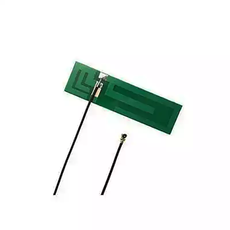
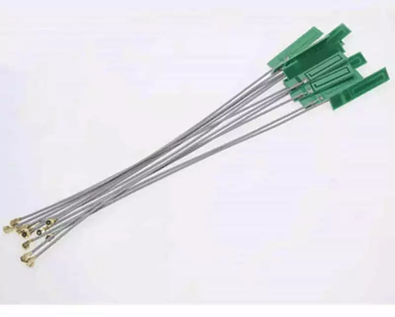
Antenna pcb, also known as pcb antenna, is antenna directly integrated onto a printed circuit board. Compared to traditional external antennas, PCB antennas achieve wireless signal transmission and reception by etching or printing specific patterns onto the PCB. This design enables seamless integration of the antenna with other electronic components within the device, saving space and enhancing the overall compactness and aesthetic appeal of the design.
Types of PCB Antennas:
Microstrip Antennas
Microstrip antennas represent a prevalent type of PCB antenna, typically comprising a planar radiating element and a ground plane separated by a layer of dielectric material. Their straightforward structure facilitates easy integration and renders them suitable for wireless communication applications across multiple frequency bands, such as Wi-Fi, Bluetooth, and cellular networks.
Strip Antenna
Strip antennas form radiating elements by etching wide conductive strips onto the PCB circuit board. Their broad bandwidth supports multi-band communication requirements, making them suitable for devices needing multi-frequency support, such as smartphones and multi-functional routers.
Loop Antenna
Loop antennas achieve radiation and reception by designing a circular structure on the PCB circuit board. Circular antennas offer high gain and excellent directionality, making them suitable for devices requiring high-performance communication, such as satellite communications and high-frequency radar systems.
Helical Antennas
Helical antennas incorporate a helical structure on the PWB, achieving radiation characteristics through multiple turns. They possess favourable polarisation properties and broadband performance, making them suitable for wireless communication systems requiring multi-polarisation support.
Considerations for PCB Antenna Material Selection:
- Dielectric Constant (Er): The dielectric constant determines signal propagation speed within the material, significantly influencing antenna dimensions, frequency response, and radiation characteristics. Optimal antenna design requires selecting an appropriate dielectric constant to meet specific frequency ranges and size requirements.
- Loss Tangent (Tan δ): This metric quantifies material loss under high-frequency signals. A lower loss tangent minimises signal attenuation and enhances antenna efficiency.
- Thermal Stability: A PCB substrate’s thermal stability is crucial for maintaining antenna performance across varying ambient temperatures. Excessive temperatures may cause board deformation or alterations in dielectric constant, thereby compromising antenna performance.
- Mechanical Strength and Machinability: PCB materials in antenna design require robust mechanical strength, particularly for structural stability under high-frequency signals. Additionally, ease of machining and surface treatment are essential considerations when selecting PCB materials.
Manufacturing of Circuit Board Antennas:
Material Selection
The performance of PCB antennas is significantly influenced by the materials chosen. Materials with high electrical conductivity, such as copper and aluminium, are typically employed for the antenna’s conductive elements to ensure efficient signal transmission. The selection of dielectric materials is critical, requiring careful consideration of their dielectric constant and loss factor to optimise the antenna’s electromagnetic performance. Typically, circuit board materials for antenna radiator designs should be relatively thick with a low dielectric constant (Dk value), such as materials with a Dk between 2.2 and 3.5.
Although materials with higher Dk values may exhibit lower radiation efficiency, antenna circuits often employ materials with a Dk of approximately 3, considering multiple factors. Organic materials include phenolic resin, glass fibre/epoxy, polyimide, and BT/epoxy, whilst inorganic materials also constitute viable substrate options. For instance, RO4534 and RO4535 represent ceramic-filled, glass cloth-reinforced thermosetting resin materials offering excellent dimensional stability and uniform mechanical properties, thereby enhancing passive intermodulation (PIM) performance. For antenna applications above 60GHz, rolled copper is the preferred copper foil, and low-loss PTFE materials should be selected for the substrate, such as DiClad 880 laminates or the RO3003 series of ceramic-filled PTFE composites.
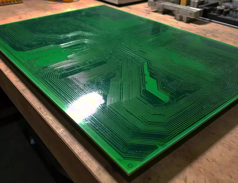
Etching and Printing
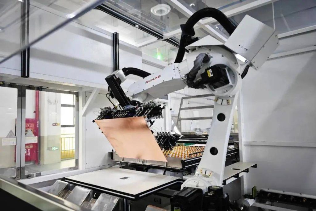
The etching or printing of antenna patterns constitutes a critical step in PCB antenna manufacturing. High-precision etching processes and advanced printing techniques ensure the accuracy and consistency of antenna patterns, thereby enhancing overall antenna performance. Etched antennas offer significant advantages in terms of high precision and robust reliability.
However, their complex manufacturing processes and higher costs render them unsuitable for structurally intricate antennas. The photochemical etching process involves applying photosensitive resist or dry film resist to a clean copper-clad laminate. This is followed by exposure, development, film hardening, and etching to form the power circuit image. Etched antennas typically utilise copper or aluminium materials, employing production techniques analogous to those for flexible printed circuit boards. A typical PCB fabrication process utilises the ‘pattern plating method’, wherein a lead-tin resist layer is pre-plated onto the copper foil sections requiring retention (the circuit pattern areas), followed by chemically etching away the remaining copper foil.
Multilayer Board Design
To achieve complex antenna structures and higher integration, PCB antennas frequently employ multilayer board designs. Signal routing and shielding between different layers enhance antenna performance and interference resistance. For instance, High-Density Interconnect (HDI) stacking allows multi-layer circuits to be connected via precisely controlled blind and buried vias, whose diameters are significantly smaller than traditional PCB through-holes. This refined interconnection method not only reduces board volume but also increases routing density.
Multilayer PCBs find extensive application in computing, meeting demands for high-speed signal transmission, stability, and integration. Higher dielectric constants in multilayer PCB materials enable smaller antenna dimensions, though this also narrows the antenna bandwidth. Ceramic antennas, possessing higher dielectric constants than PCB substrates, effectively minimise antenna size. When designing multilayer PCBs, the number of layers must be determined based on circuit scale, board dimensions, and electromagnetic compatibility (EMC) requirements.
Surface Treatment
The surface treatment of antennas significantly impacts their performance and durability. Processes such as gold plating or tin plating enhance conductivity and oxidation resistance, thereby extending the antenna’s service life. The fundamental purpose of PCB surface treatment is to ensure favourable solderability or electrical performance. This is because copper oxidises readily in air; if the copper layer oxidises, it may lead to cold solder joints, false solder joints, or even prevent pads from soldering to components.
Common PCB surface treatments include OSP (Organic Solderability Preservative), hot-dip tin plating, electroless nickel/gold plating, electroless silver plating, electroless tin plating, and electroless gold plating. Among these, OSP is a process that chemically grows an organic film layer on bare copper surfaces, offering oxidation resistance, thermal shock resistance, and moisture resistance. In millimetre-wave PCB antenna surface treatments, silver plating typically outperforms gold plating in terms of RF performance, delivering superior overall antenna effectiveness.
PCB antenna application domains:
Consumer electronics: Smartphones (5G/Wi-Fi/Bluetooth), tablets, smartwatches.
Internet of Things (IoT): Sensor nodes, RFID tags, smart home devices (e.g., ZigBee modules).
Automotive electronics: GPS navigation, keyless entry systems, in-vehicle communication modules.
Industrial and Medical: Industrial wireless control, remote monitoring devices, medical monitors.
Communications Infrastructure: 5G base station antenna arrays, small cells.
As antennas integrated onto printed circuit boards, PCB antenna plays an indispensable role in contemporary wireless communications due to their miniaturisation, high integration, and cost-effectiveness. Looking ahead, antenna pcb will continue evolving towards multifunctionality, enhanced performance, and reduced dimensions. Through innovative design methodologies and manufacturing techniques, PCB antennas are poised to achieve breakthroughs in emerging fields, further advancing wireless communication technologies and unlocking greater convenience and possibilities for modern living.