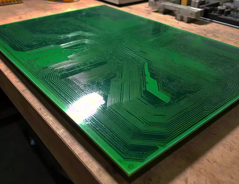
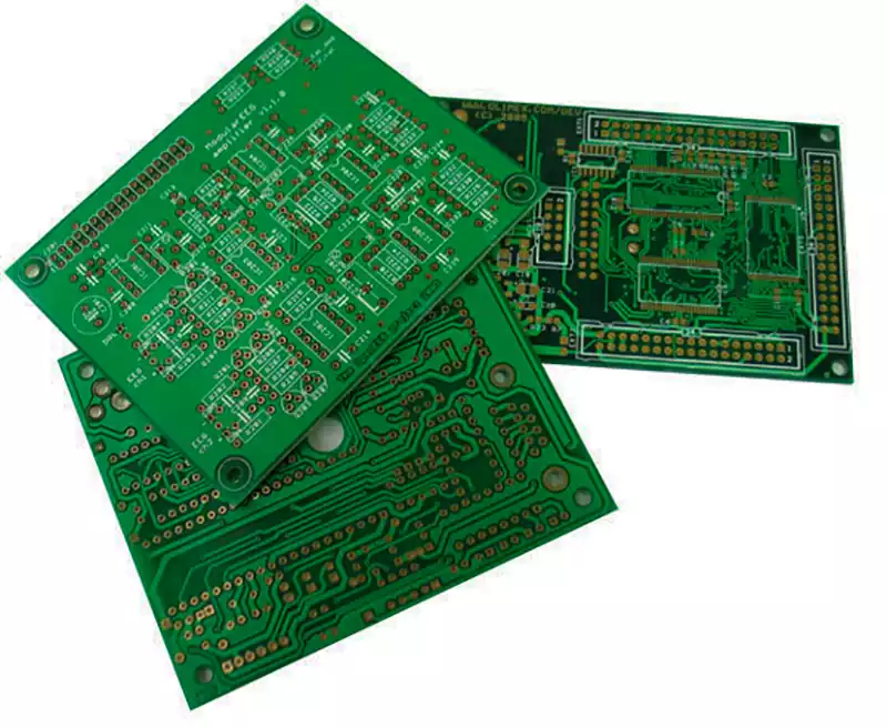
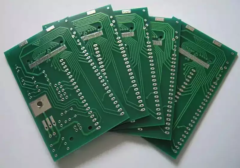
Multilayer PCB (Multilayer Printed Circuit Board) is printed circuit boards formed by alternately bonding and laminating three or more layers of conductive patterns with insulating materials. This structure not only provides electrical connectivity between layers but also achieves electrical insulation between them. Common multilayer board configurations include signal layers, internal power planes (maintaining internal power layers), and ground planes.
The number of layers in multilayer pcb is typically even—such as 4, 6, or 8 layers—as symmetrical structures help minimize warping during manufacturing processes. Electrical connections between layers are achieved through vias, which include through-holes, blind vias, and buried vias, each serving distinct interlayer connection requirements.
Basic Composition of multilayer PCBs
Multilayer PCBs adopt a sandwich-style laminated structure, alternately stacked with conductive layers, insulating layers, vias, surface finish layers and other components. Their fundamental composition consists of the following core parts:
1.Conductive Layers
Composition: High-purity copper foil (electrodeposited copper foil or rolled copper foil), which forms circuit traces after etching.
Function: Signal transmission and power distribution. Classified by functions as below:
Signal Layers: Located on the Top Layer, Bottom Layer or inner layers, used for routing signal traces and mounting electronic components.
Power Planes and Ground Planes: Arranged in inner layers. They deliver stable power supply and reference ground potential for circuits, and meanwhile provide electromagnetic shielding to mitigate interference.
2.Insulation Layers
Composition: Cores and Prepregs.
Function: Offer electrical insulation and mechanical support, and maintain consistent interlayer thickness.
Core: Rigid intermediate supporting substrate made of fiberglass fabric impregnated with epoxy resin (e.g. FR-4), clad with copper foil on both sides to provide primary mechanical strength.
Prepreg: Semi-cured epoxy resin-impregnated fiberglass fabric sandwiched between cores or copper foils. It melts and cures under high temperature and pressure during lamination, serving as bonding and filling material to guarantee electrical isolation between layers.
3.Vias
Composition: Metallized holes embedded or concealed inside the PCB circuit board with copper deposited on hole walls.
Function: Establish electrical interconnections between different conductive layers. Classified by position: through vias penetrating the entire board; blind vias connecting surface layers to inner layers; buried vias linking only inner layers.
4.Surface Finish and Auxiliary Layers
Solder Mask: Ink coating covering conductive layers except pads (commonly green). It prevents solder bridging and short circuits, and defines soldering regions.
Silkscreen Layer: Text and graphics printed onto the solder mask (usually white), marking component designators, polarity indicators, version information, etc., to facilitate component assembly and maintenance.
Surface Finish: Coating materials deposited on pads (e.g. ENIG, HASL, OSP) to avoid copper oxidation and improve solderability.
Stackup Logic
Multilayer PCBs are fabricated by alternately stacking cores, prepregs and copper foils, followed by lamination under high temperature and pressure. Metallized vias realize electrical connections between individual layers to form sophisticated multilayer interconnection structures.
Common Substrates for multilayer PCBs
1.General-Purpose Standard Substrates (Most Widely Adopted)
FR-4 (Epoxy Fiberglass Laminate): The dominant substrate for multilayer PCBs. Fabricated with fiberglass fabric reinforced epoxy resin, it features outstanding electrical insulation, high mechanical strength, favorable thermal resistance and stable dielectric properties with competitive cost performance. It is extensively applied in industrial control equipment, consumer electronics, general power supplies and most conventional multilayer PCB applications.
2.High-Frequency / High-Speed Substrates (For High-Frequency & High-Speed Scenarios)
PTFE (Polytetrafluoroethylene) Substrates: Extremely low dielectric constant (2.0–3.0) and ultra-low dissipation factor, significantly reducing signal attenuation. It is the preferred substrate for RF, microwave, satellite communication and multilayer PCBs operating above 10 GHz, though with relatively high cost.
Modified Epoxy / Hydrocarbon Resin High-Frequency Materials (e.g. RO4350, S1139): Stable dielectric constant and low dissipation factor, with machinability comparable to FR-4. Suitable for multilayer PCBs working below 3 GHz including 5G communication equipment, high-end servers and millimeter-wave radars. Its cost is slightly higher than FR-4.
3.High-Tg / High-Temperature Resistant Substrates (High-Power & High-Temperature Operating Environments)
High-Tg FR-4 (e.g. Tg150, Tg170): Improved glass transition temperature based on standard FR-4, delivering superior thermal resistance and dimensional stability. Suitable for high-power, heat-intensive or high-reliability applications such as automotive electronics, industrial control and high-layer-count PCB lamination.
Metal-Based Substrates (Aluminum Base / Copper Base PCBs): Excellent thermal conductivity, adopted for high-current and high-heat scenarios including LED lighting, new energy vehicle electronic control systems and high-power power supplies. These are special-function boards rather than mainstream conventional multilayer PCB substrates.
4.Low-Grade Low-Cost Substrates (Low-Performance Requirement Scenarios)
Paper-Based / Composite Substrates (e.g. FR-1, FR-2, CEM-1, CEM-3): Low material cost, yet inferior mechanical strength, thermal resistance and insulation performance compared with FR-4. Mainly used for low-layer-count simple boards with modest performance requirements such as small home appliances, electronic toys and low-end controllers, and rarely used in formal multilayer PCB designs.
5.Special Substrates (Special Environment & Structural Requirements)
Polyimide (PI) Substrates: Outstanding temperature resistance and flexibility, primarily applied in flexible multilayer PCBs (FPC) or rigid-flex PCBs, such as mobile phone cables, camera modules and wearable devices.
Ceramic Substrates: Combine high thermal conductivity and superior insulation performance for power semiconductor devices and high-end packaging applications. The material cost is extremely high, so its adoption in multilayer PCBs is limited.
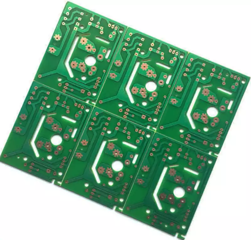
Advantages of Multilayer Circuit Boards
High Integration and Complex Design Capability
By increasing the number of internal conductive layers, multilayer PCBs enable higher-density circuit layouts within limited space, meeting the design demands of complex electronic systems. Smartphones exemplify this, where highly integrated components and intricate circuits rely on multilayer board technology for functional consolidation.
Superior Electrical Characteristic Optimization
The multilayer structure incorporates ground planes and shielding layers, significantly improving high-speed signal transmission quality. This design effectively suppresses electromagnetic interference (EMI), ensuring signal integrity for both high-frequency digital and analog circuits. Simultaneously, shorter signal paths reduce transmission delays, enhancing system response speed. Typical applications like high-speed computer motherboards rely on multilayer architectures to guarantee stable data transmission and high-speed performance.
Compact and Lightweight Design
Compared to single/double-layer boards, multilayer pcbs accommodate more circuits within the same area, thereby reducing PCB size and weight. This characteristic is particularly crucial for space-constrained devices like wearables and aerospace electronics. Take the Apple Watch Series 8 as an example: its multilayer board design integrates complex functions such as biosensing and wireless communication within a miniaturized body while maintaining lightweight properties.
Enhanced Structural Reliability
Despite manufacturing complexity, multilayer boards’ three-dimensional interconnect structure (achieved through via holes connecting layers) significantly boosts mechanical strength and vibration resistance. This structural integrity ensures stable electrical connections in harsh environments, making them ideal for reliability-critical industrial control and automotive electronics.
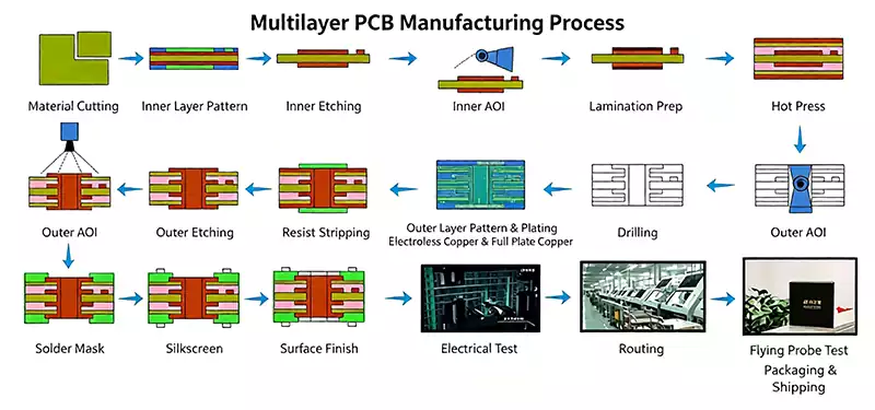
Multilayer PCB manufacturing process
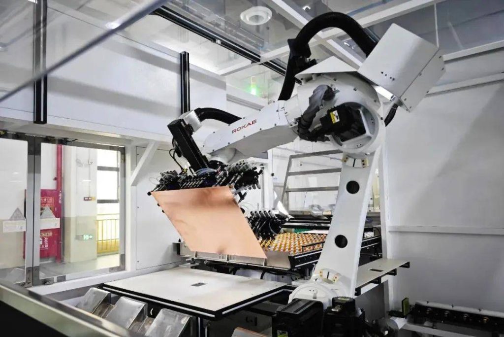
Core fabrication: Complete inner layer patterning, etching and AOI inspection for core boards.
Stack-up & lamination: Arrange cores and prepregs in designed sequence, then laminate under high temperature and pressure.
Drilling & metallization: Drill vias and conduct electroless copper plating for interlayer connection.
Outer layer fabrication: Pattern top and bottom conductive traces via exposure and etching.
Surface finish: Apply HASL, ENIG, OSP or IAg to avoid copper oxidation.
Solder mask & silkscreen: Coat solder mask and print component marking legends.
Routing & testing: Cut boards to required shape, perform electrical test, impedance check and visual inspection before delivery.
Application Fields of Multilayer PCB
The communications sector stands as one of the most critical and extensive industries for multilayer circuit board applications.
In contemporary communication devices—such as smartphones and Wi-Fi routers—multilayer PCBs have become critical components supporting technological evolution. Through three-dimensional routing design, this technology achieves high-density component integration within limited space. Simultaneously, its layered structure establishes low-impedance signal pathways, significantly boosting data transmission rates. This precisely aligns with industry trends toward miniaturization and high performance in communication equipment.
Crucially, the shielding layers and grounding systems integrated within multilayer PCBs form effective electromagnetic isolation structures, substantially mitigating external interference impacts on signal integrity. This interference resistance ensures communication link stability in complex electromagnetic environments, providing reliable hardware support for core functions like voice calls and data transmission. This directly enhances user communication quality and satisfaction.
Consumer Electronics:
From smartphones, tablets, and televisions to home appliances, nearly all consumer electronics rely on multilayer PCBs to connect and communicate between functional modules. The high-density routing and compact design of multilayer PCBs enable these devices to become thinner, lighter, and more portable while simultaneously enhancing their performance and functionality.
Automotive Electronics:
As automotive intelligence advances, an increasing number of electronic components are integrated into vehicles. Multilayer PCBs serve as the critical bridge for interconnecting and communicating between these components. Their high-temperature tolerance and vibration resistance ensure stable operation in harsh automotive environments, safeguarding the reliability of automotive electronic systems.
In industrial control applications, multilayer PCB boards are used in various controllers and automation equipment. These devices require precise control and processing of diverse signals. The high precision and reliability of multilayer PCBs meet the demanding requirements of industrial environments, ensuring stable and safe production processes.
In aerospace applications, multilayer PCBs are highly favored for their compact size, lightweight nature, and stable performance. For instance, aircraft electronic systems and navigation equipment utilize multilayer PCB boards to meet the stringent size and weight constraints of aerospace applications while ensuring reliable operation under extreme conditions.
In medical equipment, such as magnetic resonance imaging (MRI) machines and CT scanners, multilayer PCBs form core components. These devices process vast amounts of medical imaging data and complex control signals, making the high performance and stability of multilayer circuit boards critical for diagnostic accuracy and equipment safety.