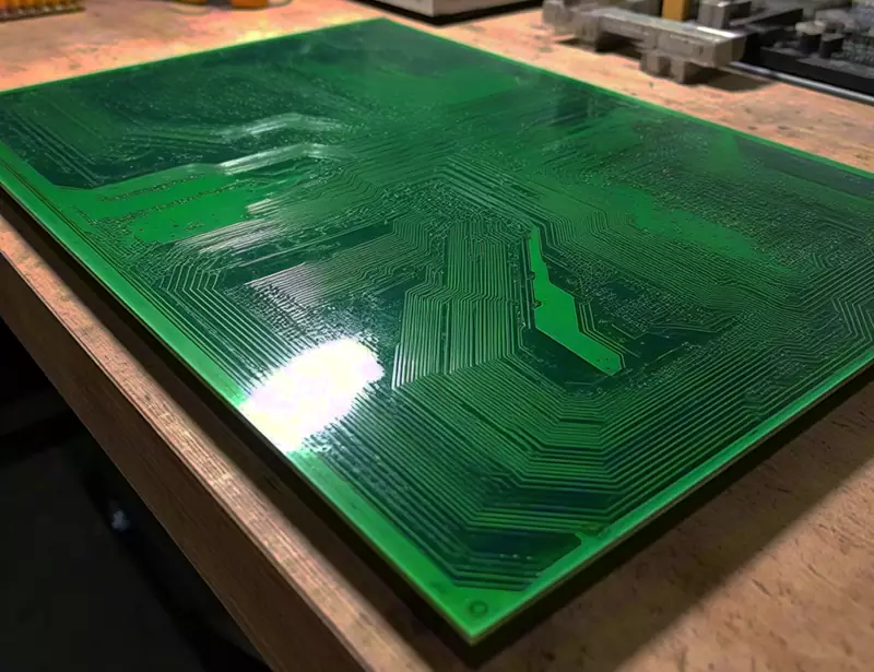
What is a PCB board? A PCB board, known in Chinese as a printed circuit board, serves as the carrier for the electrical interconnection of electronic components, acting as a relay for signal transmission. It is thus referred to as the “motherboard of electronic products.”
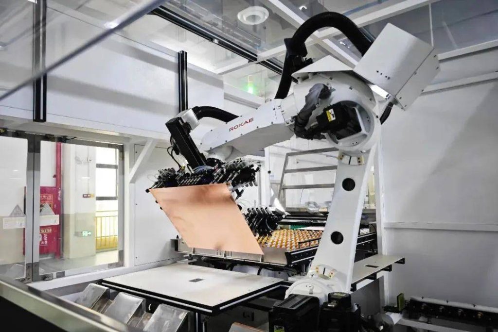
In modern electronics manufacturing, the PCB board forms the foundation for Surface Mount Technology (SMT). The core of SMT lies in precisely mounting various components—such as resistors, capacitors, and BGA chips—onto specific pads on the PCB circuit board.
This requires the pad positions and dimensions on the PCB to strictly match the component packages used in SMT. For instance, a 0402-sized resistor requires a corresponding pad dimension of 0.4mm × 0.2mm. Only by meeting such matching requirements can the SMT process proceed smoothly and ensure the quality of the final product.
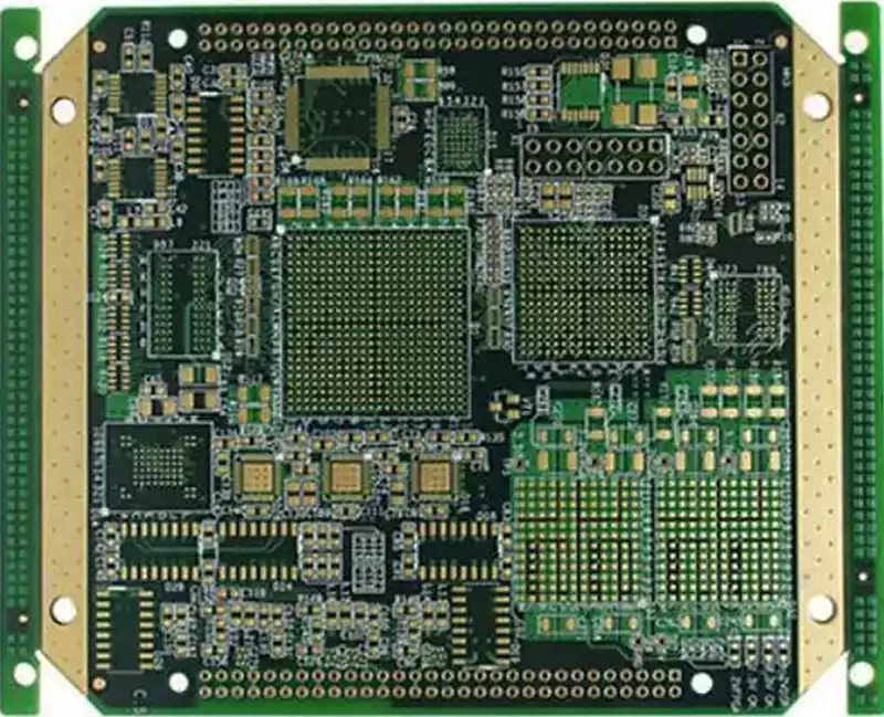
Simultaneously, the SMT process enhances the value of PCB boards. Through SMT technology, components can be mounted in high density on both sides of the PCB. This high-density mounting approach significantly drives the miniaturization of electronic devices. Take a mobile phone motherboard as an example: the BGA chip is mounted on the PCB via SMT, enabling “pinless” high-density connections. This allows for the integration of more functions within limited space, enhancing the overall performance and competitiveness of electronic devices.
PCB circuit boards are primarily categorized into the following types:
Single-Sided Boards
Single-sided boards feature components concentrated on one side of the basic PCB board, with conductive traces on the opposite side (surface-mount components share the same side as traces, while through-hole components reside on the other side). Since traces appear only on one side, this PCB circuit board is termed single-sided. Due to stringent design constraints (traces cannot cross and must follow separate paths on a single side), single-sided boards are primarily used in legacy circuits.
Double-Sided Boards
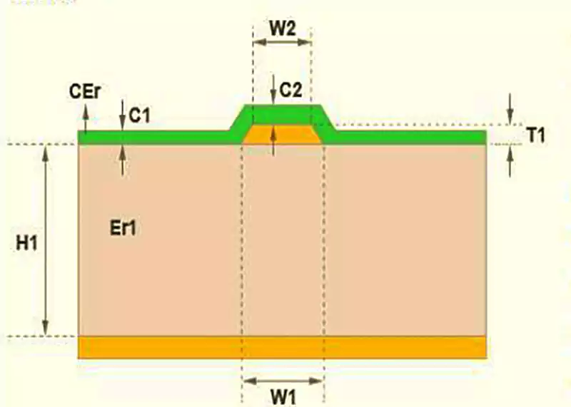
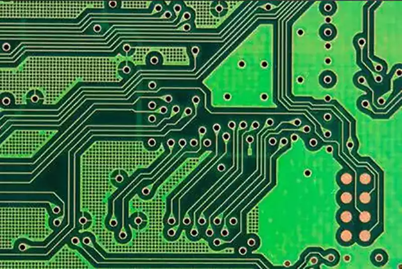
Double-sided boards feature circuit layouts covering both surfaces. However, achieving electrical connectivity across both sides relies on specific interlayer connection structures. This connection medium is called a via—essentially a micro-sized metallized through-hole machined into the PCB substrate. Through electroplating or filling with conductive material, it forms an electrical interconnection channel between the two sides.
Compared to single-sided boards, double-sided boards double the available routing area, effectively overcoming the layout bottlenecks caused by line crossings in single-sided designs. Designers can route intersecting lines through vias to the opposite side, significantly increasing circuit complexity. Due to this capability, double-sided boards have become the mainstream choice for moderately complex electronic products, widely used in circuit designs requiring more functional modules or signal interactions.
Multilayer PCB Boards
Multilayer pcb boards expand routing space by stacking multiple conductive layers. Their structure typically combines double-sided boards as inner layers with single-sided boards as outer layers (or double inner layers + double outer layers). Each layer is alternately laminated using positioning systems and insulating bonding materials, achieving conductive pattern interconnections per design specifications to form printed circuit boards with four, six, or more layers. Note that the total number of layers does not strictly equate to the number of independent routing layers—blank layers may be added in special cases to adjust board thickness.
Consequently, multilayer boards are typically designed with an even number of layers (including the two outermost layers). Current mainstream motherboards predominantly use 4 to 8-layer structures. While PCB layers can theoretically reach nearly a hundred, in practical applications, although ultra-high-layer motherboards were once widely used in large supercomputers, such ultra-multilayer boards have gradually exited the mainstream market with the popularization of cluster computing technology. Due to the tight bonding of PCB board layers, the number of layers is difficult to discern directly with the naked eye, but it can still be roughly determined by observing the motherboard cross-section.
PCB Board Layer Classification and Functions:
Signal Layers
Top Layer and Bottom Layer: Used for routing and component placement, these are the most fundamental conductive layers in a PCB circuit board.
Mechanical Layers
Mechanical Layer: Defines mechanical structural information such as PCB board dimensions and mounting hole positions, possessing no electrical properties. Typically, up to 16 mechanical layers can be configured.
Silkscreen Layers
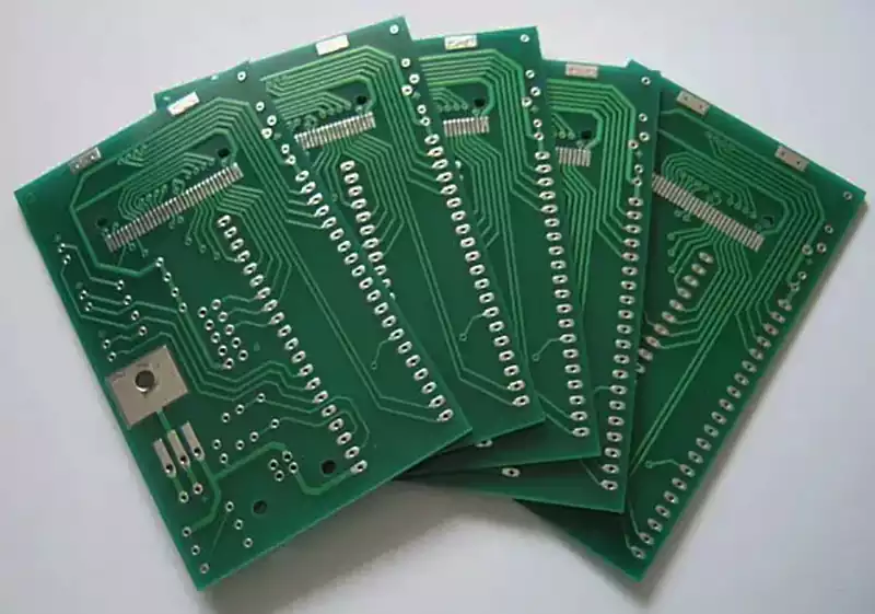
Top Overlay and Bottom Overlay: Used to mark component numbers, annotations, logos, and other assembly information. Typically white and applied via screen printing.
Paste Layers
Top Paste and Bottom Paste: Used to indicate pad locations requiring solder paste application during SMT (Surface Mount Technology) processes. These are critical layers for surface mount soldering.
Drill Layers
Drill Grid and Drill Drawing: Provide drilling information for PCB manufacturing, including the positions and dimensions of drill holes for vias, pads, etc.
Keep Out Layer
Defines non-routable areas such as PCB board edges, slots, and cutouts, restricting the placement of traces and components to ensure circuit design integrity and safety.
Multi Layer
Multi Layer is an abstract layer representing electrical connection paths for components requiring penetration through the entire PCB circuit board (e.g., through-hole pads, vias). Graphics on this layer appear across all conductive layers (except Plane layers), typically defining plated-through holes (PTH) or non-plated-through holes (NPTH).
How to Design a PCB Circuit Board
PCB design constitutes a critical development phase within product hardware engineering, serving as the vital link between schematic design and physical pcb circuit board fabrication. The project workflow is as follows:
1) Project initiation requires verification of complete documentation: Schematics, structural diagrams, component libraries, signal flow diagrams for complex products, power tree diagrams, critical signal specifications, power/current requirements, and design constraints.
2) Design data input: Import netlists and structural diagrams. After importing the structural diagram, pay special attention to screw hole and positioning hole dimensions, component and trace no-placement zones, height-restricted areas, and connector locations.
3) Layout: Place components rationally on the board while comprehensively considering requirements for signal integrity, EMC, thermal design, DFM, DFT, structural integrity, and safety regulations. The fundamental approach to placement, beyond structural constraints, primarily involves aligning with signal flow and power flow directions.
4) Routing Constraints: Routing constraints primarily include trace width, spacing, and length matching. Some rules require pre-simulation guidance, such as trace length, impedance, topology, and stackup structure.
5) Routing: Routing constitutes the most labor-intensive phase of PCB design, demanding attention to numerous factors. These include trace impedance, ground plane continuity, EMC, SI/PI, and DFM.
6) Review + Post-Simulation Verification: Upon completing routing, senior personnel must conduct a review and inspection, followed by simulation verification of critical signals and power planes.
7) Fabrication: Once the PCB design is finalized, photoplotting files can be output for production.
As the core carrier of electronic products, the design and manufacturing quality of PCB boards directly determine product performance and reliability. Looking ahead, with the proliferation of 5G, artificial intelligence, and IoT technologies, PCB circuit boards will evolve toward higher layer counts, finer line widths, and high-frequency/high-speed materials (such as low-loss PTFE). Simultaneously, they must meet stringent certification standards for sectors like automotive electronics and medical devices.