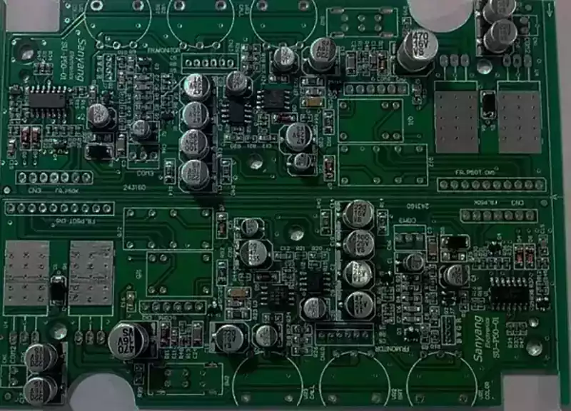
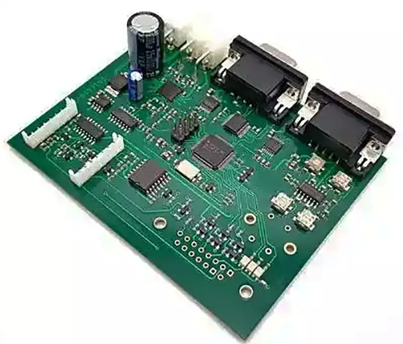
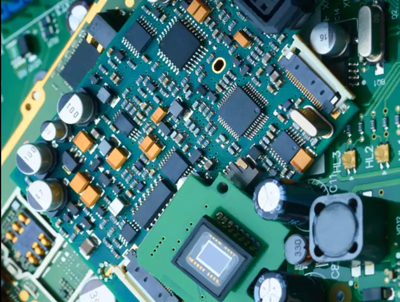
What is PCBA? PCBA stands for Printed Circuit Board Assembly. It is not merely a simple printed circuit board (PCB), but rather involves mounting electronic components (such as surface-mount devices SMT and through-hole components DIP) onto the PCB board and forming a complete circuit system through processes like soldering.
What is the difference between PCB and PCBA?
A PCB is the raw, unpopulated circuit board, while a PCB assembly is the finished circuit ready for immediate operation. A PCB focuses on the physical design of circuit paths, whereas a PCBA is the functional circuit that incorporates components. A simple mnemonic is: PCB + Components + Soldering = PCBA. In fact, a PCB circuit board assembly cannot exist without a PCB—the PCB is the first step, and the PCB assembly is built upon it.
Key Differences Between PCB and PCB Assembly:
| Aspect | PCB Board | PCB Assembly |
| Definition | Circuit boards with exposed, unmounted components providing electrical connections | A printed circuit board with electronic components assembled upon it constitutes a functional circuit. |
| Function | Mechanical support and electrical pathways for components | Perform specific electronic functions |
| Component | None (blank circuit board) | All necessary electronic components (resistors, capacitors, integrated circuits, etc.) |
| Appearance | A planar circuit board featuring conductive traces, pads and vias | A pcba board equipped with various electronic components |
| Manufacturing | Etch the copper layer on the substrate; Apply the solder mask layer. | Place and solder components onto the PCB (Surface Mount Technology, Through-Hole Technology) |
| Testing | Continuity and Short-Circuit Testing of Copper Wiring | Comprehensive testing (ICT, functional testing) to ensure proper operation |
| Stage | Base/Pedestal | Completed/Functional circuitry |
| Application | For use in the early design stages, prototyping and circuit validation | For end products such as smartphones, computers and industrial electronics |
What is PCBA manufacturing? The PCBA production process involves multiple sequential steps to complete manufacturing, primarily divided into several major workflows: SMT assembly → DIP insertion → PCBA testing → conformal coating.
Circuit board assembly Process Flow:
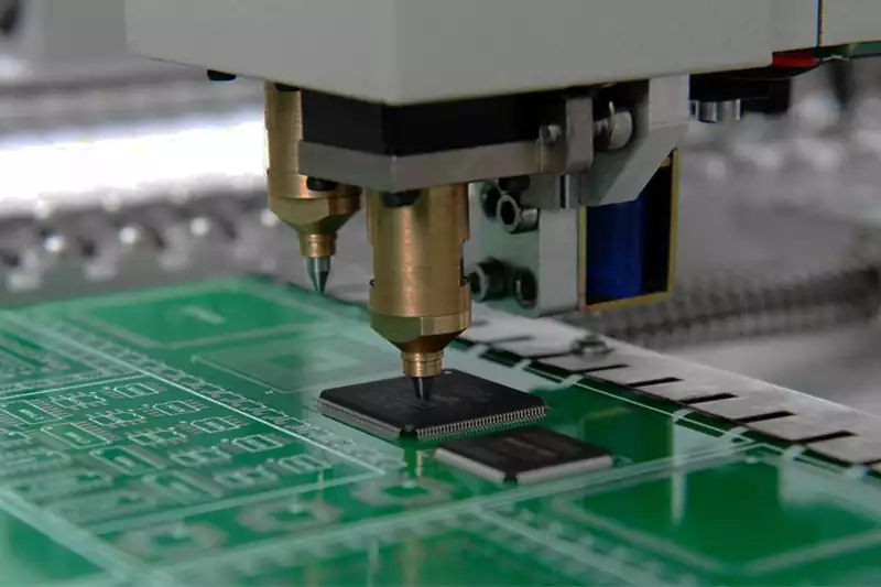
SMT Assembly
SMT assembly is the initial step in PCB assembly production, encompassing multiple precision operations: First, refrigerated solder paste must be thawed. Once restored to room temperature, it is thoroughly mixed manually or via automated stirring equipment to ensure paste homogeneity meets printing standards. The processed solder paste is then evenly applied to the stencil surface.
Guided by the directional scraping action of a squeegee, the paste is precisely deposited through the stencil apertures onto the designated pads on the PCB. Immediately after printing, SPI (Surface Mount Inspection) equipment performs three-dimensional thickness inspection. This equipment monitors critical parameters such as solder paste volume, height, and offset in real time, providing data support for process control.
During the component placement phase, high-speed pick-and-place machines precisely identify electronic components in feeder magazines via vision systems, achieving high-precision placement at rates of tens to hundreds of components per second with positioning accuracy of ±0.05mm. The assembled PCB boards then proceed to the reflow soldering process.
Within a nitrogen-protected heating environment, they traverse four temperature zones: preheating, soaking, reflow, and cooling. This sequence induces phase transitions in the solder paste—drying, melting, wetting, and solidification—ultimately forming reliable intermetallic compound bonds. Post-soldering, the entire board undergoes AOI (Automated Optical Inspection) using multi-spectral imaging technology for non-contact verification of component placement, polarity, coplanarity, and solder quality, achieving inspection accuracy at the 5μm level.
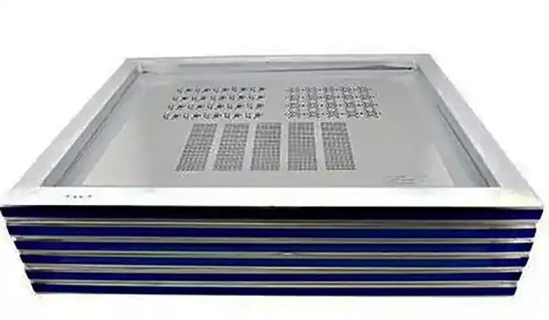
Defects such as bridging, tombstoning, or misalignment detected by AOI require manual or automated rework at dedicated stations. The rework process includes component removal, pad cleaning, re-placement, and secondary soldering. Hot-air rework stations enable damage-free desoldering through precise temperature control. The entire SMT production process must be conducted within a Class 10,000 cleanroom, maintaining an ambient temperature of 23±3°C and humidity at 45%±10% RH to ensure soldering quality and product reliability.
DIP Component Assembly
The DIP component assembly process encompasses several critical stages, including insertion, wave soldering, lead trimming, post-soldering processing, board cleaning, and quality inspection. These steps collectively form the complete DIP assembly workflow.
PCBA Testing
PCBA testing covers multiple aspects, including ICT testing, FCT testing, ageing tests, and vibration testing. These testing methods directly impact the product’s overall performance and quality. For instance, ICT testing primarily examines component soldering integrity and circuit continuity to ensure soldering quality. Conversely, FCT testing focuses on comprehensive verification of the PCBA board’s input and output parameters, confirming compliance with design specifications and performance metrics. Through these tests, we ensure each PCBA board meets predetermined quality standards, laying a robust foundation for subsequent production stages.
PCBA Conformal Coating
As a core process safeguarding electronic circuit reliability, PCBA conformal coating significantly enhances circuit board resistance to environmental corrosion by forming a protective layer. This process employs a stepwise application method: first, uniform spraying is applied to one side (Side A) of the PCB board assembly, followed by a pre-curing stage to achieve initial surface drying. After flipping the circuit board, the same process is applied to the opposite side (Side B). The coating is then fully cured through 24 hours of natural curing at ambient temperature.
During implementation, a laser thickness gauge continuously monitors coating thickness to ensure it remains within the 100-300μm process window. Environmental control systems maintain strict parameters of ≥16°C temperature and <75% relative humidity within the work area, supplemented by a dust-free purification system (cleanliness grade ≥ISO Class 7) to prevent particulate contamination. PCBs subjected to this triple-protection treatment achieve outstanding comprehensive performance: breakdown voltage increases to ≥5kV, water absorption rate decreases to <0.5%, and no leakage occurs even after 72 hours under high-temperature/high-humidity conditions (85°C/85% RH). This makes them particularly suitable for demanding applications such as automotive electronics and industrial control systems.
PCBA testing procedures are typically tailored to client-specific test plans, with the fundamental workflow comprising:
Programming → ICT Testing → FCT Testing → Ageing Testing
- Programming
Following front-end soldering operations, engineers commence programming microcontrollers within the PCB board assembly to enable specific functionalities. - ICT Testing
ICT testing primarily employs test probes contacting the PCBA’s test points to verify circuit continuity, detect short circuits, and assess component soldering integrity. This method offers high accuracy, clear indications, and broad applicability. - FCT Testing
FCT testing evaluates environmental parameters, electrical characteristics (current/voltage), and mechanical stresses (pressure) on the circuit board assembly. This comprehensive assessment ensures all board parameters meet the designer’s specifications. - Ageing Test
The ageing test simulates user scenarios by continuously powering the PCBA board without interruption. This detects hard-to-identify defects and evaluates the product’s lifespan, ensuring its stability.
Following a series of PCBA testing, PCBA boards that pass inspection may be labelled as compliant. They are then packaged and dispatched.