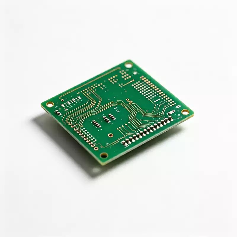
A PCB via is a plated hole that connects copper on different layers of the board. Any board with more than one layer uses vias to move a signal from the top surface down to an inner layer, to link inner layers together, and to anchor components in place. A via is as basic to the board as a pad or a trace. The trace carries a signal within one layer, and the via carries it from one layer to the next.
What are the main PCB via types
A via does two jobs: it makes the electrical connection between layers, and it holds components in place. By process, there are three kinds: through-hole, blind, and buried vias.
| Type | Structure | Connects | Process complexity | Cost |
|---|---|---|---|---|
| Through-hole via | Drills through every layer | Top to bottom, full board | Low | Low |
| Blind | Drills from a surface layer to a set inner layer, stops short | Surface to inner | Medium | Medium |
| Buried | Sits entirely inside the board, invisible from the surface | Inner to inner | High | High |
The through-hole via runs from the top surface all the way to the bottom. It is the most mature process and the cheapest, and it is what the vast majority of boards use today. A blind via stops at a chosen inner layer; a buried via never reaches the surface at all. Neither one takes up surface space, which makes them central to high-density and HDI boards, at the cost of more process steps and tighter layer-count limits.
From a design view, a via is sized by two parts: the drill hole in the middle and the pad around it. On fast, dense boards, designers always want the hole smaller, because smaller means more routing room and lower parasitic capacitance, which suits high speed. But a hole cannot shrink forever. It is limited from both sides by drilling and plating: the smaller the hole, the longer the drill time and the easier it wanders off center; once the hole depth passes six times its diameter, the barrel can no longer be plated with even copper. A six-layer board is about 50 mil thick through its through-holes, so the smallest drill a fabricator can offer lands at 8 mil.
Should PCB vias be as small as possible
Smaller vias save board space, but that line of thinking only goes half way. The real cost lives in plating yield.
A through-hole via with an aspect ratio above 6:1 makes copper plating and chemistry exchange difficult, and the barrel copper comes out uneven, which is where reliability testing starts failing. Sacrificing yield for a slightly smaller hole is the most common false economy on high-speed boards.
Some vias should never be shrunk. Power vias carry far more current than signal vias, and their hole diameter is usually more than double a signal via’s, or the temperature rise and current load become unmanageable. Ground vias sit densely around high-speed signals to provide a return path, and their size and count come straight from simulation rather than from habit.
High-speed PCB via rules for stubs and backdrilling
Push the data rate up and the via suddenly becomes the number one signal-integrity headache. The problem is not the hole itself. It is the stub.
A through-hole via that runs the full thickness of the board, used by a high-speed signal to change layers at only a few of those layers, leaves the unused copper barrel hanging in the layers the signal never reaches. That dead length of metal is called a stub. It is an open-circuited transmission line dangling at the end, and it causes three things: impedance discontinuity that reflects the signal, resonance at certain frequencies that swallows signal energy, and insertion loss that shrinks the eye diagram and drives up bit errors.
The numbers are ugly. A 60 mil (about 1.5 mm) stub adds roughly 8 dB of extra loss to a 25 Gbps signal and can sink an otherwise qualified link entirely. On FR-4, a 0.5 mm stub resonates around 10 to 12 GHz, right in the Nyquist band of many 25 Gbps channels. The stub also brings parasitic capacitance of about 0.5 to 1 pF per millimeter and parasitic inductance of 0.3 to 0.5 nH per millimeter, enough to pull a designed 100 ohm differential impedance down to 70 or 80 ohms.
The fix is backdrilling. A normal through-hole is drilled, copper-flashed, and fully plated; backdrilling comes after plating and uses a larger drill bit from the back of the board to remove the idle copper barrel, leaving only the short section the signal actually uses. The backdrill bit runs 0.15 to 0.2 mm larger than the original hole, so a standard 0.2 mm via needs a 0.45 to 0.55 mm backdrill bit. The leftover can never be zero: standard process leaves 4 to 6 mil of residual stub, and demanding zero just scraps the batch.
Which pcb boards must be backdrilled: high-speed SerDes differential signals above 8 Gbps, including PCIe 4.0 and 5.0, USB4, and 10G, 25G, and 56G Ethernet, wherever a through-hole change leaves a long stub; the clock, address, and data lines of DDR4 and DDR5; any layer-changing via whose signal runs inner but whose hole pokes through to the back with nothing on it, the classic high-speed crash zone; and thick boards over 2.0 mm, where the total via length multiplies the stub problem.
When backdrilling is unnecessary: low-speed signals in the low Mbps range, where the stub is negligible; through-holes that use every layer with no idle section; HDI blind and buried vias, which have no long stub by construction; and simulated short stubs under 8 to 10 mil, which can be exempted. Blanket backdrilling across the whole board only adds 15 to 30 percent cost and lowers reliability for nothing.
Backdrilling is not a note in the fab file that says please backdrill the high-speed vias. The design side has hard requirements. The production document must name four things: the backdrill start side, the stop layer, the maximum allowed residual stub, and the net list involved. Backdrill the high-speed vias is too vague to mean anything. The larger backdrill bit means every inner and stop layer it passes needs an enlarged antipad to clear the drill and stop it scoring inner copper into a short.
Backdrill vias must also clear component pads by at least the usual 0.2 mm safety gap, or the drill tears the pad copper directly. Blind and buried vias are off limits for backdrilling; that remedy belongs to through-holes only. And the stub tolerance has to be confirmed by simulation, because tolerance needs differ sharply by data rate and stack-up. Guessing from experience ends in trouble.
The higher the rate, the harder the stub budget. At 112G and 224G links the stub has to sit inside 4 ± 2 mil. Above 20 GHz the backdrill stub already matters; at 30 GHz the insertion-loss gap between different stub lengths is dramatic. HFSS simulations give a slightly counterintuitive result: a 4 mil stub and a 0 mil stub are nearly identical in return loss, but pad diameter matters just as much, a 18 mil pad behaving like a 20 mil pad plus zero stub. So optimizing the via means shrinking the pad along with the stub, not staring at the stub alone.
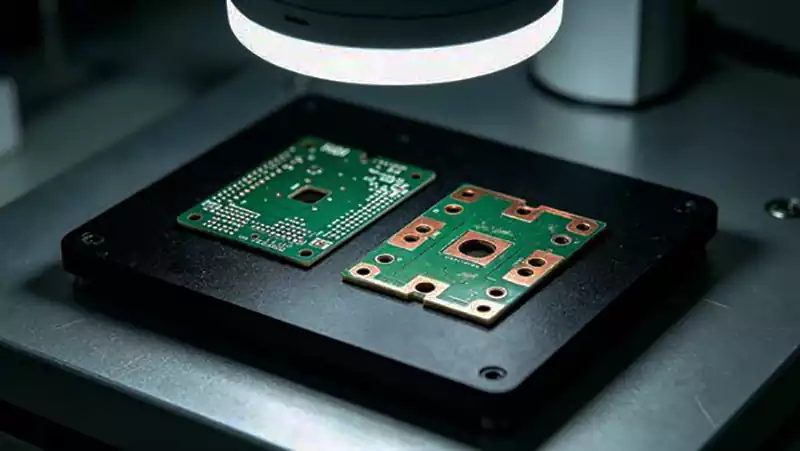
Choosing between backdrilling and HDI blind vias
Both backdrilling and HDI blind vias exist to kill the stub, and picking the wrong one wastes money.
Backdrilling keeps the standard through-hole and adds a second drilling step. Its upside is that it works with ordinary laminates, needs no HDI process, and slips into an existing design with little redesign. The downside is the 4 to 6 mil residual stub that remains, the ±2 to 4 mil backdrill tolerance, the antipad overhead, and the 15 to 30 percent added cost.
HDI blind vias change layers with almost no stub and give the best signal integrity of the options, most visibly in dense BGA fanout. The cost is the HDI process itself, a stack-up planned from the start, tight space under the BGA, and a higher price.
The engineering priority is clear: if HDI blind vias are available, use them first and remove the stub at the source; where an existing design cannot reach HDI because of cost or process, backdrilling is the patch; and the best answer of all is to place high-speed layer changes close to the board surface during stack-up planning, shortening the idle stub and cutting the backdrill volume before it exists.
Frequently asked questions about PCB via types
How many PCB via types are there? Three. A through-hole via runs the full board thickness. A blind via links a surface layer to an inner layer. A buried via links inner layers only. The ones that do not run the full thickness are the blind and buried vias; the one that takes no surface space is the buried via.
What is the difference between a blind via and a buried via? A blind via is drilled from a surface layer, usually the top or bottom, down to a chosen inner layer, and its opening shows on the surface. A buried via sits entirely between inner layers and cannot be seen from outside. Both serve HDI and high-density designs; blind vias fit where surface routing is tight, and buried vias fit where inner-layer density is the constraint.
When is backdrilling mandatory? For high-speed SerDes above 8 Gbps, DDR4 and DDR5 clock, address, and data lines, layer-changing vias that hang open at the back, and thick boards over 2.0 mm. It is not needed for low-speed signals, through-holes that use every layer, HDI blind and buried vias, or simulated short stubs under 8 to 10 mil.
Do vias affect signal quality? Yes. Vias carry parasitic capacitance and inductance, and high-speed signals also need a return path. The idle section of a via that is not part of the signal connection forms a stub, which at high speed causes resonance and worsening insertion loss, and that is exactly why backdrilling exists.
Can backdrilling reach zero stub? Mechanical backdrilling cannot. Standard process leaves 4 to 6 mil of residual stub, and 112G-and-up links ask for 4 ± 2 mil. True zero stub comes from HDI blind-via layer changes, or from depth-controlled electrical testing, a higher-tier process that is not yet widespread.
PCB Via selection comes down to what the pcb board actually needs. A two- to four-layer board is fine with through-holes run top to bottom. Past 8 Gbps the stub loss and reflection have to be reined in with HDI blind vias or backdrilling. Where the BGA is dense and routing is tight, blind and buried vias are the only option that pays. Before the stack-up is finalized, walk every high-speed signal through its layer-changing vias: which layers it uses, which it leaves idle, and how long that idle section is. Skip that half hour and the backdrill count and the yield points stop being yours to decide.