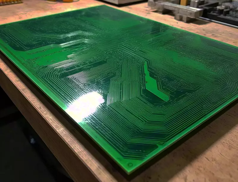
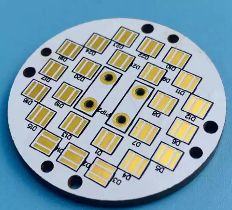
Manufacturing yield of a multilayer PCB is the share of boards in a batch that pass from panel cutting to finished goods on the first attempt. More layers mean a longer process chain, and every step adds cumulative dimensional error and another chance for defects. Compared with single- and double-sided boards, yield pressure on a multilayer PCB sits where it cannot be seen. Inner-layer circuits are sealed inside during lamination, and layer misregistration or inner-layer shorts are hard to repair at the finished stage, so process control has to catch them earlier.
Low yield costs most on high-layer boards. These are usually system boards with large panels and high unit value. When an inner-layer short is found after lamination, the whole batch may be scrapped together. Boards with weak hole-wall plating look acceptable at first assembly, then develop barrel cracks and open circuits after a few thermal cycles, which moves the loss to the customer. Rework and full inspection can sort out part of the bad output, but both cost and delivery time grow.
Yield of a multilayer PCB is set by several steps working together. Inner-layer imaging and core expansion set the registration baseline, lamination stacking joins the layers, drilling and hole metallization build the interlayer connections, and process inspection catches defects along the chain. Deviation at any step adds up and shows up in final layer registration and electrical continuity.
Inner-layer imaging sets the registration baseline of a multilayer PCB
Inner-layer circuits are formed before lamination, so imaging accuracy sets the registration base after pressing. Conventional film exposure holds image registration at about 25 micrometres and interlayer registration above 50 micrometres, which tends to shift patterns on high-layer boards. Laser direct imaging brings interlayer pattern accuracy within 12.7 micrometres. Another process data set gives pattern registration around 15 micrometres and interlayer registration within 30 micrometres. High-layer boards generally control interlayer registration tolerance around 75 micrometres, and imaging accuracy is the main variable inside that budget.
Checks after etching matter as much as exposure. Each etched core is measured at independent targets for expansion and contraction. In one eight-layer trial, the spread of core expansion was 0.0406 millimetres in X and 0.0417 millimetres in Y, inside the control range. Engineering practice keeps core-to-core dimensional deviation within 50 micrometres, and a value beyond that calls for an adjustment to the compensation factor. Trace width and pads need allowance at the design stage. Special patterns such as looped traces, isolated lines and impedance lines get their own compensation checks, and first-article approval comes before volume production.
Core expansion compensation sets layer consistency in a multilayer PCB
Cores in a multilayer PCB do not expand and contract in the same way. Material direction, copper distribution and earlier thermal cycles all change dimensions. Compensation factors are built up from production data and then used to correct pattern size layer by layer, so that registration after lamination stays inside tolerance. Different laminates and prepregs carry different expansion coefficients, and a new material or a first use of a special material calls for process validation.
Expansion control runs through several steps. After cutting, the number of sheets per stack is set by core thickness, and stacks are laid flat for pre-baking. After lamination, a post-bake cures the material and lets its state settle before drilling. Incomplete cure leaves sticky chips during drilling, blocks flute clearance and can break the bit. Imaging or drilling a panel that still holds heat from an earlier step also introduces dimensional error, so newer lines insert a timed buffer after each thermal process.
Lamination registration controls layer shift in a multilayer PCB
Lamination stacks cores and prepreg into a board, and it is the step where layer shift is easiest to introduce. Common pre-registration methods use four-slot tooling, hot melt, riveting, or hot melt combined with riveting. High-layer boards usually take four-slot tooling or fusion plus riveting. Tooling holes are punched to within 25 micrometres and must be free of offset, ovality and burrs. Riveted stacks are checked for concentricity before pressing, and only stacks inside the limit enter the press.
The press cycle follows the material. With several cores and prepregs stacked together, a fast temperature rise or a poorly timed pressure change causes layer slide, delamination, voids and trapped air. High-layer boards slow the heating rate and extend the high-temperature cure so the resin flows and fills completely. One pressure schedule uses 100 to 120 degrees Celsius at 50 to 100 psi for pre-press, then 170 to 200 degrees Celsius at 200 to 400 psi for 60 to 120 minutes in the main press, with cooling below 50 degrees Celsius to lock the structure. Laminates with different Tg values cannot share a press load, and standard boards cannot be pressed together with boards that need special parameters.
The stack structure itself has to serve yield. A dielectric layer that is too thick pushes the finished board over thickness, and one that is too thin invites delamination and failure at high-voltage test. Interlayer dielectric thickness is generally held within 10 percent, with tighter grades for impedance boards. High-resin prepreg fills gaps between traces on heavy copper boards, but a full stack of high-flow fine-glass prepreg weakens dimensional stability, so it is mixed with other styles.
Drilling accuracy sets hole position quality in a multilayer PCB
Drilling is the main yield risk on high-layer boards. Many layers, accumulated copper and greater panel thickness wear bits quickly and cause breakage, while tight wall-to-wall spacing in dense areas brings ion migration failures. At 14 layers and above, or with hole diameter at 0.2 millimetres or less, or hole-to-trace distance at 0.175 millimetres or less, drills with position accuracy within 0.025 millimetres are used. A thickness-to-diameter ratio of 12 to 1 calls for step drilling and drilling from both faces, and holes above 4 millimetres are also machined in steps.
Bit condition decides hole wall quality. Bit material needs a fine grain structure, the shank-to-edge diameter tolerance sits between 0 and 0.005 millimetres, and concentricity stays within 0.005 millimetres. Flute length is set at 1.15 times the stack thickness plus the entry depth into the backing board, with at least 15 percent of the flute left outside the board for chip clearance.
A single bit on a multilayer PCB is normally limited to 1500 holes, then replaced or reground. High-layer work uses new bits or bits reground once. One heavy-copper trial held regrinds to three or fewer to reduce burrs. An entry cover reduces inlet burrs and bit breakage, a backing board protects the exit side and the table, and drilling depth is set in steps by bit diameter.
Hole wall roughness is usually held within 25 micrometres. A rough wall, pits in the substrate and resin smear weaken the continuity of later electroless copper and leave plating voids. During drilling the bit can reach over 200 degrees Celsius, and softened resin is carried onto the copper foil edge of the wall as smear, which must be removed before hole metallization.
Plating quality sets interconnect reliability in a multilayer PCB
Plated holes join the layers, and hole-wall copper is central to the quality of a multilayer PCB. An acceptable deposit has suitable thickness, uniformity and ductility, and survives 10 seconds at 288 degrees Celsius without cracking. A crack in thermal shock opens circuits between inner layers and between inner and outer layers, ranging from intermittent conduction to a scrapped board.
Wall preparation comes before plating. Desmear removes melted resin and drill debris, and etch-back removes non-metallic dielectric in a controlled way so inner-layer conductors project into the hole and form a three-dimensional bond with the plated copper. Etch-back depth is generally 5 to 10 micrometres. Micro-etching roughens the surface for electroless copper, and a rate of 0.7 to 0.9 micrometres per minute is needed to keep the wall copper from cracking under thermal shock.
Plating uniformity is hardest on fine-pitch traces, 14 to 20 layers, and small holes at thickness-to-diameter ratios of 6 to 1 through 10 to 1. Methods include a low-copper, high-acid bath with a sulfate-to-copper concentration ratio above 10 to 1, lower cathode current density with longer plating time, and vertical oscillation added to cathode movement and air agitation so the bath exchanges inside small holes and the thickness gap between hole mouth and centre narrows. Voids are traced by their shape. Bath concentration, rinse water temperature, activator, trapped air and brush pressure each produce a distinct pattern, and each cause is checked in turn.
Process inspection sets where defects are caught in a multilayer PCB
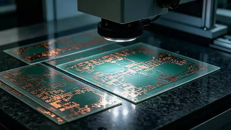
Yield control puts inspection at the step where a defect is created and stops bad work at the source. Many hidden defects in a multilayer PCB are sealed in during lamination. Sampling inner layers alone leaves shorts and residual copper for the press stage, and the batch may be scrapped. Full automatic optical inspection of every inner panel before lamination catches routing faults early.
The etching step needs timed calibration. After more than ten hours of continuous running, copper ion concentration in the chemistry rises and the etch rate slows, so the first half of a batch meets trace width while the second half leaves fine copper bridges between lines that are hard to see. Sampling bath concentration and trace width every two hours and adjusting at once keeps etching defects down. Drilling relies on enforced bit life and spindle accuracy checks.
Layer shift after pressing is checked by X-ray, and the first fused panel is approved before a batch starts. During production each panel is checked for correct fusion into the unit to prevent later delamination. For hidden layer bonds and hole walls, thermal stress testing combined with cross-sectioning is a common method. One high-layer group was held at a solder melting condition of 217 degrees Celsius for 50 to 90 seconds, then judged against the relevant standard. Failure analysis runs from non-destructive to destructive: X-ray and ultrasonic scanning locate the fault, then metallographic cross-sections confirm wall bonding and crack paths.
Checkpoints for multilayer PCB manufacturing yield
- Use high-accuracy imaging for inner-layer patterns, measure target expansion after etching, and keep core-to-core deviation within 50 micrometres.
- Build compensation factors from laminate and prepreg behaviour, validate new or special materials first, and leave settling time after each thermal step.
- Confirm tooling hole accuracy and rivet concentricity before lamination, set heating and pressure curves by material, and keep laminates of different Tg in separate press loads.
- Select drilling equipment by layer count and hole size, limit regrinds and hole count per bit, hold wall roughness under 25 micrometres, and use entry and backing boards.
- Control desmear and etch-back depth, hold micro-etch rate at 0.7 to 0.9 micrometres per minute, and verify plating with thermal shock.
- Run full optical inspection on inner layers before pressing, sample bath and trace width every two hours, and check layer shift by X-ray after lamination.
- Set reliability conditions from the soldering profile of high-layer boards, locate faults with non-destructive methods, then confirm by cross-section.
Common questions about multilayer PCB manufacturing yield
Why is layer registration so hard on high-layer boards?
More layers mean more reference points. Exposure alignment, hole punching, core expansion, lamination tooling and drilling accuracy each contribute deviation, and these deviations add up on a high-layer board. Interlayer registration tolerance is usually around 75 micrometres, and it takes accurate imaging, expansion compensation and a suitable lamination registration method together to hold it.
Why inspect inner layers fully before lamination?
After pressing, inner-layer circuits are sealed inside the board. Shorts and residual copper are hard to locate at the finished stage and have no economical repair route. Full optical inspection before lamination stops those faults early and avoids an irreversible loss of the whole batch.
Why replace a drill by hole count?
A worn bit produces rough walls, burrs and resin smear, which lead to plating voids and barrel cracking after thermal cycling. Setting a hole-count limit by material and panel thickness, then replacing or regrinding on schedule, costs less than tracing a defect after it appears.
Manufacturing yield of a multilayer PCB is managed in process order. First get inner-layer imaging and expansion compensation accurate, then control lamination registration and the press cycle, then hold drilling and hole metallization quality, and use process inspection to catch defects at each step. Once these points stay stable, layer registration and interconnect reliability have a base to rest on.