What is HDI PCB? HDI PCB (High-Density Interconnect Printed Circuit Board) is a type of high-density interconnect printed circuit board. HDI stands for “High Density Interconnect.” HDI PCB achieves higher wiring density and smaller dimensions through advanced manufacturing techniques and design methodologies. Compared to traditional PCBs, the most significant feature of HDI circuit boards lies in their ability to achieve higher-density circuit layouts and connections.
Core Characteristics and Technologies of HDI
Microvia Technology: This is the most fundamental hallmark of HDI.
Laser Drilling: Primarily uses UV or CO2 lasers to drill microvias (Microvia) with diameters typically less than 150µm (commonly 50-100µm) on extremely thin dielectric layers.
Blind/Buried Vias: HDI extensively employs blind vias (connecting outer and inner layers without traversing the entire board) and buried vias (connecting only inner layers without extending to outer layers). This significantly frees up surface layer space for routing.
Stacked/Staggered Vias: To connect more layers, HDI employs stacked vias (multiple microvias stacked vertically) or staggered vias (multiple microvias arranged in an offset pattern). Stacked via processes are more complex and costly but offer shorter interconnect paths.
Fine Lines and Spacing: Line widths and spacings are significantly reduced, typically below 100µm (commonly 50-75µm or even lower). More advanced photolithography techniques (such as semi-additive process/mSAP) are employed to achieve such fine line dimensions.
High Routing Density: The combination of microvias and fine lines substantially increases the number of conductors that can be routed per unit area, enabling high-density interconnections for complex circuits.
Thin Dielectric Materials: Utilizing thinner (e.g., ≤50µm) high-performance copper-clad laminates (CCL) and prepregs, along with low-profile copper foil, forms the foundation for achieving ultra-thin interlayer structures and fine traces.
Increased Layer Count and Any-Layer Interconnection: HDI pcbs readily accommodate higher layer counts (8+ layers are common). Cutting-edge Any Layer Interconnect (ELIC) technology enables connections between any layers via microvias, delivering maximum design flexibility.
Advanced Surface Finishes: Options like ENEPIG (Electroless Nickel-Electroless Palladium-Gold), electroless silver, electroless tin, and OSP meet solder reliability requirements for high-density pads and fine-pitch components.
Advantages of HDI PCB boards:
HDI boards utilize micro blind vias and buried vias to achieve multi-layer high-density stacking, significantly enhancing routing density. Micro-aperture and high-precision laser drilling ensure precise circuit connections, shorten signal paths, reduce signal loss and crosstalk, and guarantee signal integrity.
Maximized Space Utilization
HDI technology saves PCB board area through blind/buried vias, enabling thinner, lighter, and smaller device designs to meet stringent size and weight requirements of modern electronics.
High-Speed Signal Transmission Assurance
Low-dielectric-constant materials and optimized laminate structures reduce signal delay, enhancing transmission stability and reliability for high-speed signals.
High Reliability and Durability
Multi-layer lamination and precision manufacturing ensure robust structures, adapting to complex environments and extending product lifespan.
Enhanced Design Flexibility
Supports more complex circuit designs and functional integration, meeting diverse demands for high-performance electronics.
HDI PCB Laminate Structure:
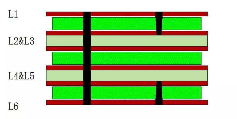
Single-Layer-Up Printed Circuit Board (Single-Layer-Up 6-layer board, laminate structure: (1+4+1))
This HDI board structure is the simplest, as the inner multilayer boards contain no buried vias, requiring only a single lamination to complete manufacturing. Although classified as a single-layer laminate, its manufacturing process closely resembles the single-lamination process for conventional multilayer boards. The primary difference lies in subsequent steps, such as laser drilling of blind vias.
Since this laminate structure does not involve buried vias, the second and third layers can be fabricated as one core board, while the fourth and fifth layers form another core board. Subsequently, dielectric layers and copper foil are added to the outer layers, followed by interlayer dielectric insertion before a single-pass lamination. This method is highly straightforward and offers lower costs compared to conventional single-pass laminated boards.
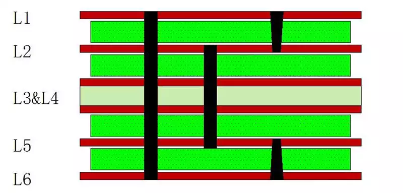
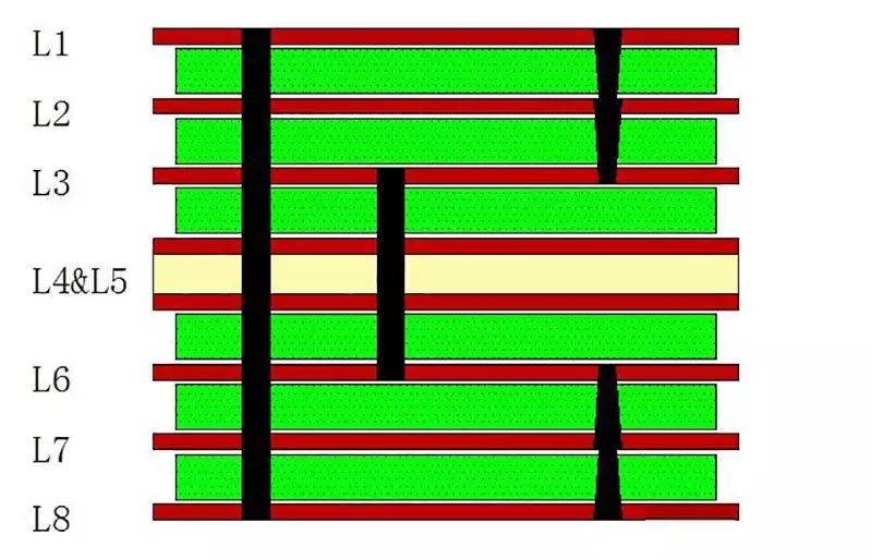
Single-Laminate Printed Circuit Board (Single-Laminate 6-Layer Board, Laminate Structure: (1+4+1))
The structure of this HDI board is typically represented as (1+N+1), where N≥2 and N is an even number. This design represents the mainstream single-laminate board structure in the current industry. Its internal multilayer board incorporates buried vias and requires secondary lamination to complete. Beyond blind vias, this single-layer laminate also incorporates buried vias. Converting such HDI boards to simpler Class I single-layer laminates benefits both suppliers and customers. Many clients have adopted recommendations to optimize conventional Class II single-layer laminate stackups into structures resembling simpler Class I single-layer designs.
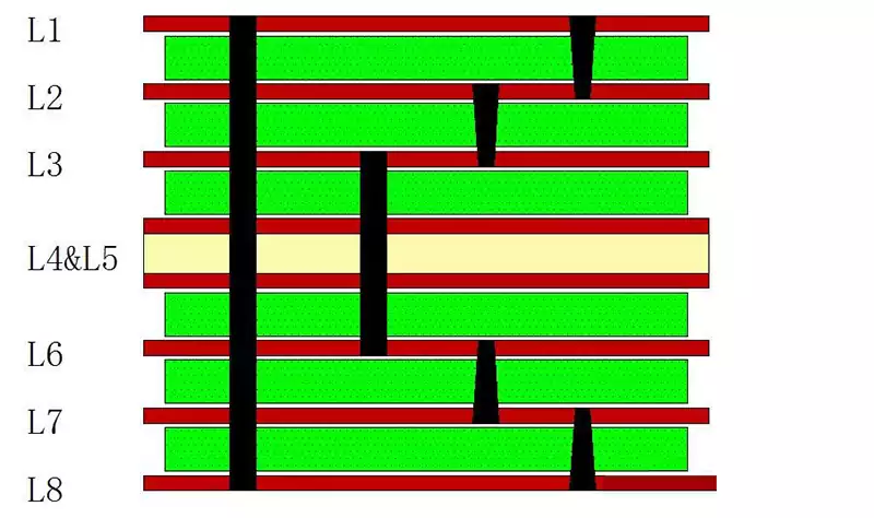
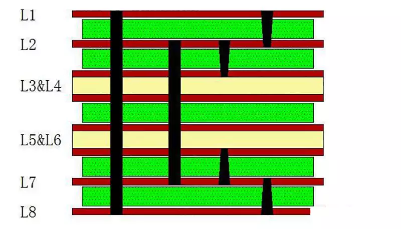
Conventional secondary-laminated HDI pcbs (e.g., 8-layer secondary-laminated HDI with a stackup of (1+1+4+1+1))
This HDI board structure follows the format (1+1+N+1+1), where N≥2 and N is an even number. It represents the current industry standard for secondary-laminated designs. The internal multilayer board contains buried vias, necessitating a triple-lamination process for completion. The primary characteristic of this design is the absence of stacked vias, resulting in standard manufacturing complexity. Optimizing the placement of buried vias from layers (3-6) to layers (2-7) would eliminate one lamination process, thereby streamlining production and achieving cost reduction.
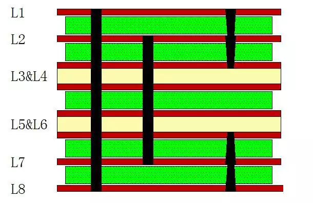
Conventional double-stacked HDI printed circuit boards (double-stacked HDI 8-layer board, stacked structure: (1+1+4+1+1))
This HDI board structure is (1+1+N+1+1), where N≥2 and N is an even number, representing a secondary laminated board configuration. Despite this, because buried vias are placed between layers (2-7) rather than (3-6), this design optimizes the secondary laminated HDI board from a three-press process to a two-press process. Another manufacturing challenge for this board lies in its (1-3) layer blind vias, which necessitate splitting them into (1-2) layer and (2-3) layer blind vias for fabrication. Specifically, the internal blind vias in layers (2-3) necessitate via filling technology for completion. This implies that the internal blind vias in the secondary laminate must be fabricated using via filling.
Typically, HDI pcbs employing via filling incur significantly higher costs and manufacturing complexity compared to boards without this process. Therefore, for conventional secondary laminated boards, it is advisable to avoid stacked via designs during the design process. Instead, the (1-3) blind vias should be converted into staggered (1-2) blind vias and (2-3) buried (blind) vias. Experienced designers often utilize this simplified design approach to reduce manufacturing costs.
For double-stacked HDI pcb boards with stacked blind hole design, buried holes (2-7) are stacked above blind holes. (Double-stacked 8-layer HDI board with a stacked structure of (1+1+4+1+1))
The structure of such boards is (1+1+N+1+1), where N≥2 and is an even number, representing a current design characteristic for some double-stacked boards in the industry. The inner multilayer boards of these assemblies contain buried vias and require secondary lamination to complete. Key features include stacked via design and cross-layer blind via design.
Additionally, this design mandates stacking blind vias above buried vias on layers (2-7), increasing manufacturing complexity. Positioning buried vias on layers (2-7) reduces primary lamination steps, streamlines production, and achieves cost reduction.
The secondary laminated HDI with cross-layer blind via design (8-layer secondary laminated HDI board, stacked structure: (1+1+4+1+1))
This type of board structure, (1+1+N+1+1) (where N≥2 and is an even number), represents one of the more challenging secondary laminated boards to manufacture in the industry. This design typically incorporates buried vias between layers (3-6) of the inner multilayer board, requiring three lamination processes to complete. The primary challenge lies in cross-layer blind via design, which increases manufacturing complexity.
This makes it difficult for HDI PCB manufacturers lacking specific technical capabilities to produce such secondary laminated boards. Optimizing the cross-layer blind vias between layers (1-3) by splitting them into (1-2) and (2-3) layers—using staggered blind vias instead of stacked vias—significantly reduces manufacturing costs and streamlines production processes.
Factors Influencing HDI PCB Pricing:
Layer Count and Cost
The number of layers is a key determinant of PCB pricing. Higher layer counts necessitate more complex manufacturing processes, driving up costs. For instance, common 4- to 8-layer HDI PCBs typically range from 300 to 800 RMB per square meter. Multi-layer boards exceeding 10 layers may exceed 1000 RMB per square meter. Generally, higher layer counts correspond to higher base prices for HDI PCBs.
Line Width/Spacing and Microvia Size
Line width/spacing and microvia dimensions significantly impact HDI PCB pricing. When line width/spacing reaches smaller specifications like 2.5/2.5 mil, manufacturing complexity increases, resulting in higher costs compared to standard 3/3 mil. Additionally, smaller microvia diameters correspondingly raise production expenses. For example, vias smaller than 0.25mm typically incur additional charges from most PCB manufacturers, as drill bit penetration depth per pass drastically decreases, reducing production efficiency. Microvias are commonly laser-processed, with typical drilling dimensions ranging from 3-5mil, where 4mil is the standard design and production size.
Order Quantity
Order quantity is a key factor affecting HDI PCB pricing. Mass production leverages economies of scale to reduce per-unit costs. Generally, larger order quantities result in lower unit costs. Small-batch prototyping typically carries higher prices because fixed costs like engineering fees (approximately 300-500 RMB) and film charges (100 RMB per layer) must be spread across fewer units. In contrast, large-volume orders may see price reductions ranging from 10% to 30%.