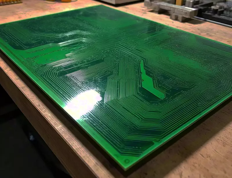
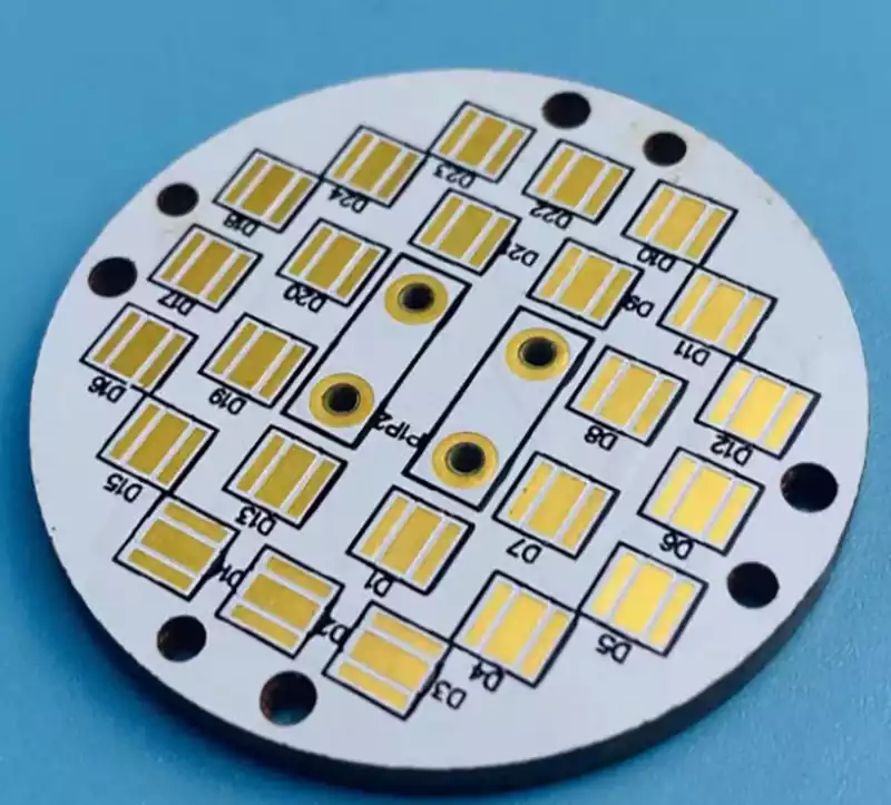
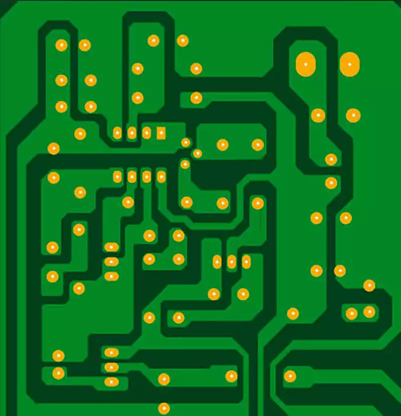
A multilayer PCB is built by pressing two base materials in alternation: cores clad with copper on one or both sides, and prepreg sheets placed between them. A core is fully cured, rigid stock with a fixed thickness and stable properties that carries the mechanical structure. Prepreg sits at an intermediate cure stage; heat and pressure soften its resin so it flows and bonds the surrounding layers, and its dielectric behavior settles close to that of the core after cooling. Material selection is the task of fixing the grade and combination of both materials against signal speed, board thickness, heat resistance and cost.
Choosing the wrong materials tends to surface only after lamination or assembly. Resin content that does not match the line spacing leaves starved edges or voids between layers. A grade or weave-direction mismatch in the prepreg on the two sides of a core builds uneven stress and warps the whole multilayer PCB. Carrying GHz-range signals on conventional stock lets insertion loss accumulate along long routes and tightens the receiver eye. Because these problems are expensive to correct after the fact, material decisions belong before the stackup is frozen and need to be checked against the fabricator’s process capability.
Four parameter groups govern multilayer PCB material selection. Dielectric constant and dissipation factor set propagation speed and attenuation. Glass transition temperature sets the heat limit. The resin content and flow of the prepreg set how well lamination fills the pattern. The way cores and prepreg are paired sets thickness and structural symmetry.
A multilayer PCB is built from cores and prepreg
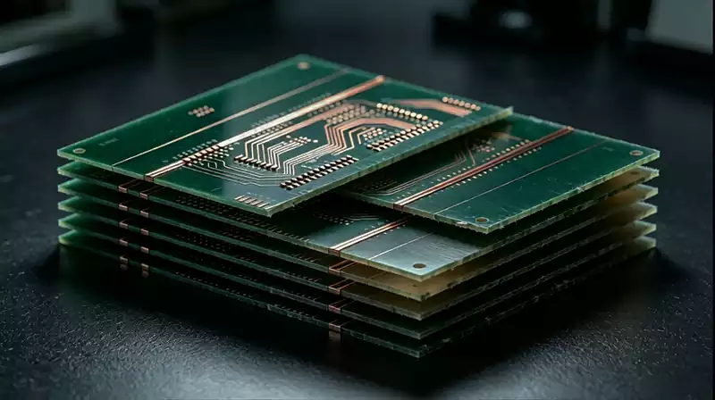
Cores are fully cured, copper-clad sheets with fixed thickness and dielectric constant, and they form the skeleton of a multilayer PCB. Outer-layer base copper on a conventional multilayer PCB is often 1/3 oz or 0.5 oz and is built up by later plating, while inner layers usually use 1 oz foil. Prepreg is made by impregnating glass cloth with resin and drying it to a partial cure; it is placed between core and copper or between two cores, softening and flowing to fill the gaps in the pattern during lamination before crosslinking into a solid. A six-layer board sometimes adds an extra core for balance when thickness and process limits require it, an arrangement known in the trade as a false eight-layer construction.
Glass cloth is the reinforcement inside prepreg, and its weave density and fiber diameter vary by style. The general rule is that a higher style number means coarser glass and a thicker dielectric layer after pressing. The distribution of gaps within the cloth affects signal transmission, an effect known in the industry as glass weave effect; uneven distribution causes propagation delay and loss variation, which matters most in high frequency multilayer PCBs.
Among common styles, 106 gives about 50 μm pressed thickness and roughly 70% resin content, 1080 about 60 to 70 μm and roughly 60%, 2116 about 90 to 110 μm and roughly 50%, and 7628 about 170 to 190 μm and roughly 45%. High-speed routing layers favor finer glass styles to reduce the effect of the weave on impedance.
Prepreg style sets dielectric thickness in a multilayer PCB
Dielectric thickness directly affects characteristic impedance, and it follows from both the style and the number of prepreg sheets. Engineers estimate a sheet count from the target thickness and then correct it with test coupons: the count is roughly the target dielectric thickness divided by the pressed thickness of one sheet. For a 7628 cloth, one pressed sheet is about 0.18 mm; with a target inner-layer dielectric of 0.2 mm the calculation gives about 1.1 sheets, so two are used. Residual copper ratio changes the result, because more open pattern area draws more resin into the gaps and leaves the finished board thinner than predicted. When residual copper exceeds 70%, the usual correction is to add 10% to 15% resin content or one extra prepreg sheet.
Standard thicknesses for a conventional multilayer PCB include 0.6, 0.8, 1.0, 1.27, 1.56, 1.6, 2.0, 2.4, 3.0 and 4.0 mm, with 1.6 mm the most common. Boards up to twelve layers generally use 1.6 mm, while higher layer counts or boards carrying large currents use 2.0 mm. Pressed thickness often comes in slightly under the design value, so a 1.6 mm target landing near 1.56 mm is within normal tolerance.
Resin content and flow govern lamination quality in a multilayer PCB
Prepreg selection for a multilayer PCB rests on four parameters: resin content, resin flow, gel time and volatile content. Resin content is the share of resin in the total prepreg weight, typically 50% to 70% for conventional boards and 45% to 50% for high-frequency low-loss boards; within one style, higher content means a thicker pressed layer and higher cost.
Resin flow is the fraction that can move during pressing, with typical test values between 15 and 30; flow that is too high starves the board edges, while flow that is too low fails to fill line gaps and leaves bubbles and voids. Gel time is the window during which the resin stays fluid enough to flow, and a short window can trap air inside the board. Volatile content is the share of components lost on drying, and excess volatiles generate gas during pressing that leads to delamination and voids.
Resin content targets vary by application. A conventional four-layer board takes 55% to 60%, balancing fill against thickness control. Heavy-copper boards with wide line gaps take 60% to 65%. High-density interconnect boards with microvias take 50% to 55%, limiting resin flow so the vias do not fill. High-frequency low-loss boards take 45% to 50% to reduce dielectric loss. Low-loss resin systems are intrinsically harder to fill and offer a narrower process window than conventional epoxy, so yield typically ramps more slowly when they enter production.
The lamination profile has to be timed against the resin. A typical vacuum press ramps at 2 to 5 ℃ per minute, with 3 to 5 ℃ suitable for conventional epoxy. Ramping too fast cures the resin before it can flow and leaves poor fill; ramping too slowly prevents air from escaping the glass gaps and creates white spots. High pressure is applied when the material reaches 70 to 100 ℃, at which point the resin has softened. Cure runs at 170 to 190 ℃ under 200 to 500 psi for 30 to 120 minutes, with vacuum held below -0.098 MPa. Applying pressure too early catches resin that is still stiff, and applying it too late catches resin that has already cured; neither case allows proper consolidation.
Prepreg is a semi-finished product with a shelf life, and storage directly affects multilayer PCB lamination yield. Sealed packs taken from cold storage need at least eight hours to warm before opening. Sheets cut to size that sit longer than three days must be rechecked before use. Cut sheets belong in a vacuum cabinet for moisture removal, and blank dimensions are increased by about 10 mm in each direction. Moisture in prepreg turns to vapor during pressing and produces both bubbles and white spots, often appearing as scattered micro-voids in a cross section and easy to mistake for a resin flow problem.
Multilayer PCB material selection starts with Dk and Df
Once signal speed enters the GHz range, dielectric constant and dissipation factor become the first criteria in multilayer PCB material selection. Dielectric constant sets propagation speed and the starting point for impedance calculation; dissipation factor sets how quickly the signal attenuates. Standard epoxy glass stock measures about 4.2 to 4.6 in dielectric constant and 0.010 to 0.020 in dissipation factor, suiting ordinary digital circuits.
Mid-range stock measures about 3.7 to 4.0 and 0.005 to 0.008, used for DDR3, DDR4 and gigabit Ethernet. High-speed stock measures about 3.3 to 3.6 and 0.002 to 0.004, matching DDR5, PCIe 5.0 and 25G serial links. Ultra-low-loss stock measures about 3.2 to 3.5 and 0.001 to 0.002, aimed at PCIe 6.0 and links above 56G. PTFE-based substrates can go as low as 2.1 to 3.0 in dielectric constant and serve millimeter-wave and phased-array antennas.
Selection depends on stability across frequency, temperature and humidity as well as the absolute value of the dielectric constant. Shifts in dielectric constant bring impedance change and delay drift, and high-speed links need it to stay consistent across a broad band. A lower dielectric constant gives faster propagation and less line delay, but it also changes characteristic impedance and has to be calculated together with the stackup.
Dissipation factor is the more critical term at high speed: with the same dielectric constant, doubling the dissipation factor makes a visible difference to signal quality at the far end of a long route. Standard epoxy glass stock sees its dielectric constant fall with frequency at 10 GHz and carries a relatively high dissipation factor, so long routes need a move to low-loss material.
Glass transition temperature sets the heat limit of a multilayer PCB
Glass transition temperature is the upper limit at which a laminate stays rigid. Above it, the material shifts from a glassy to a rubbery state and loses mechanical strength and electrical performance. Conventional epoxy glass stock sits around 130 to 140 ℃, mid-grade around 150 ℃, and high-grade above 170 ℃. Lead-free soldering requires a decomposition temperature above 340 ℃ and a glass transition temperature above 170 ℃, so boards exposed to high heat or frequent thermal cycling need a high-transition material.
Heat resistance also bears on dimensional stability and layer-to-layer registration. Stock with a low transition temperature is more prone to delamination and warpage after repeated reflow, especially in thick and high-layer-count boards. Beyond temperature, the coefficient of thermal expansion affects through-hole reliability and layer registration, moisture absorption affects dielectric stability at high frequency, and the comparative tracking index sets creepage distance in high-voltage settings. Automotive and high-reliability applications also check flame rating, CTI and relevant certifications together, so material choice rests on the full set of requirements.
Hybrid stackups cut cost but add risk to a multilayer PCB
Pure high-speed material costs several times as much as conventional epoxy glass stock and is less forgiving to process. If only a few layers of a ten layer pcb board carry signals above 56G and the rest are power and low-speed control, using high-speed material throughout wastes most of it. A hybrid stackup assigns low-loss material to the high-speed signal layers and conventional stock to power, low-speed signal and outer-adjacent layers. Material cost drops by 30% to 50%, and the established lamination process can still be used.
The difficulty in a hybrid multilayer PCB lies in material compatibility. Dielectric constants differ, around 3.0 to 3.5 for high-speed layers and 4.2 to 4.5 for conventional stock, so impedance steps appear at the interfaces and need simulation to compensate. Signals should stay off routes that pass from a high-speed layer into conventional stock and back; where that cannot be avoided, anti-pads can be optimized or backdrilling used to remove the stub.
The two materials need close coefficients of thermal expansion and cure temperatures, and their glass transition temperatures generally sit in the same band, otherwise lamination tends to delaminate or shift between layers. Low-loss resin has a smoother surface and bonds less strongly to the brown oxide layer, so interlayer adhesion needs separate verification; conventional stock, for its part, performs better against conductive anodic filament growth and suits humid, high-voltage environments.
Checkpoints for multilayer PCB material selection
- Set the dielectric constant and dissipation factor grade from the highest signal rate and operating frequency, then check laminate thickness and copper foil specification.
- Estimate prepreg sheet count from the target dielectric thickness, correct it with residual copper ratio, and confirm pressed thickness with the fabricator.
- Choose resin content and flow together: low content with high flow tends to starve board edges, while high content needs enough flow to fill fully.
- Keep prepreg grade, sheet count and weave direction symmetric on both sides of a core to avoid warpage from uneven cooling stress.
- Select transition temperature by soldering process and operating temperature; for lead-free processing check a decomposition temperature above 340 ℃ and transition temperature above 170 ℃.
- Before mixing materials, confirm that transition temperature, thermal expansion and lamination cycle are compatible, and simulate interface impedance.
- Warm and dry prepreg to storage requirements, and recheck lots that are past shelf life or have absorbed moisture.
Multilayer PCB material selection questions
Does a more expensive laminate always perform better? Not necessarily. Selection is about whether the dielectric constant, dissipation factor and transition temperature match the signal rate, power and temperature at hand. Moving a board that already works on conventional epoxy glass up to a high-frequency material adds cost and processing difficulty without benefit. Performance follows the fit between material grade and circuit demand.
Is higher or lower resin content in prepreg better? It depends on line spacing and the stackup target. Printed circuit boards with wide gaps and high residual copper need more resin to fill and take higher content; high-frequency low-loss boards take 45% to 50% to cut dielectric loss. Content also has to be paired with flow: content that is low while flow is high leaves starved edges once the resin has run off.
What needs attention when mixing high-frequency and conventional stock in a multilayer PCB?Check the impedance step from the dielectric constant difference, whether the two resins have close thermal expansion and transition temperatures, and whether one lamination cycle can serve both. Keep signals on the high-speed layers where possible, treat layer changes with anti-pads and stubs according to simulation, and verify insertion loss and impedance on first-article production boards.
Multilayer PCB material selection runs in a set order: fix the dielectric constant and dissipation factor grade from signal rate and frequency, work back from thickness and impedance targets to the core and prepreg grade and sheet count, then check resin content, transition temperature and hybrid compatibility against the fabricator’s process capability. Settling these steps before the stackup is frozen keeps material problems out of lamination and prototype builds.