What is PCB impedance? PCB impedance refers to the impedance between conductors, transmission lines, or components on a pcb board. In high-speed digital circuits and radio-frequency circuits, the precise control of PCB impedance is one of the key factors in ensuring signal transmission quality. When different signal lines propagate through a PCB, they are influenced by factors such as PCB material, trace width, trace spacing, layer spacing, and ambient temperature, resulting in distinct impedance characteristics.
Impedance (Z) represents the total resistance of a circuit to alternating current signals, determined collectively by resistance, capacitance, and inductance, measured in ohms (Ω). In direct current circuits, resistance is the primary impedance factor; however, in high-frequency alternating current circuits, capacitance and inductance exert greater influence. Parasitic capacitance between lines ‘stores’ signal energy, while the inductance of conductors ‘resists’ changes in current flow. Together, these elements constitute impedance.
For PCB boards, common impedances include 50Ω (for RF signals), 75Ω (for video signals), and 100Ω (for differential signals). These values are not arbitrarily chosen but represent ‘agreed standards’ determined by the characteristics of chips and connectors. For instance, RF chips typically feature an output impedance of 50Ω. Only when PCB traces also maintain 50Ω impedance can signal energy be transmitted with maximum efficiency, minimising reflection losses.
Impedance Classification
(1) Single-Ended Impedance: The impedance measured on a single signal trace (commonly used);
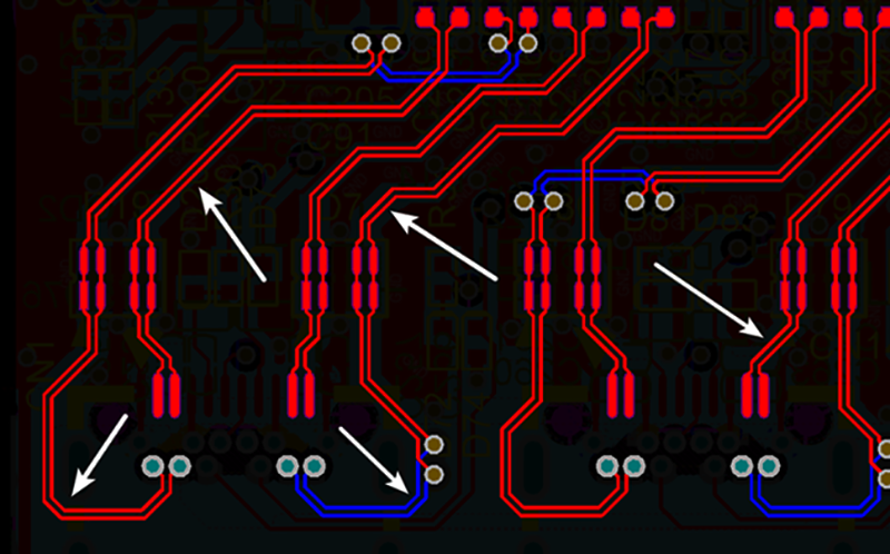
(2) Differential Impedance: The impedance measured between two transmission lines of equal width and spaced equidistantly during differential drive (commonly used);
(3) Coplanar Impedance: The impedance measured when a signal line transmits between its surrounding GND/VCC planes (uncommon).
Factors affecting impedance:
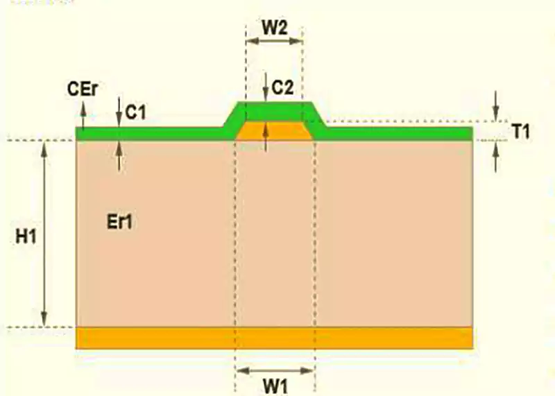
- Impedance line width: Impedance is inversely proportional to line width. A finer line width results in higher impedance, while a coarser line width yields lower impedance.
- Dielectric thickness: Impedance is directly proportional to dielectric thickness. A thicker dielectric results in higher impedance, while a thinner dielectric yields lower impedance.
- Dielectric constant of impedance: The dielectric constant is inversely proportional to impedance. A higher dielectric constant results in lower impedance, while a lower dielectric constant leads to higher impedance.
- Solder mask thickness: Solder mask thickness is inversely proportional to impedance. Within a certain thickness range, thicker solder mask results in lower impedance, while thinner solder mask leads to higher impedance.
- Copper Foil Thickness: Copper foil thickness is inversely proportional to impedance. Greater copper thickness yields lower impedance, while thinner copper results in higher impedance.
- Differential Impedance: Spacing is directly proportional to impedance. Wider spacing increases impedance, with other influencing factors being identical to those affecting characteristic impedance.
- Coplanar Impedance: Impedance is directly proportional to the distance between conductors. A greater distance results in higher impedance. Other influencing factors are identical to those for characteristic impedance.
Key Parameters Affecting PCB Impedance Calculation
The core of PCB impedance calculation lies in quantifying the impact of physical structure and material properties on impedance. Key parameters can be categorised into four groups, where even minor variations in these parameters may cause impedance fluctuations.
Transmission Line Geometric Parameters
Line Width (W): Line width significantly influences impedance. For single-ended lines, increasing width reduces characteristic impedance. For instance, raising the width of a microstrip line from 0.2mm to 0.4mm may decrease characteristic impedance 𝑍₀ from 60Ω to 40Ω. For differential lines, increasing trace spacing (S) elevates differential impedance. For instance, increasing the trace spacing from 0.3mm to 0.5mm may raise the differential impedance 𝑍𝑑𝑖𝑓𝑓 from 90Ω to 110Ω.
Dielectric Thickness (H): Dielectric thickness denotes the distance between the transmission line and the reference plane (ground/power plane). Increasing the dielectric thickness typically raises the impedance. For instance, increasing the microstrip line dielectric thickness from 0.1mm to 0.2mm may raise 𝑍₀ from 50Ω to 65Ω.
Copper Foil Thickness (T): Copper foil thickness also influences impedance. Thicker copper foil generally reduces the skin effect’s impact, but impedance decreases slightly. For instance, changing from 1oz to 3oz copper foil may reduce 𝑍₀ from 50Ω to 48Ω.
Dielectric Material Parameters
Dielectric Constant (Er): The dielectric constant is a key indicator for dielectric materials. Generally, the higher the dielectric constant of a material, the slower the signal propagation speed and the lower the impedance. For the common PCB substrate FR-4, its relative dielectric constant at room temperature and 1GHz frequency is approximately 4.2–4.8. High-frequency substrates such as Rogers RO4350 exhibit a relative permittivity of approximately 3.48, making them suitable for high-frequency applications like 5G RF. Note that permittivity varies with frequency; for instance, FR-4’s permittivity drops to 3.8 at 10GHz. Neglecting frequency characteristics may introduce calculation errors.
Reference Plane Design Parameters
Reference plane integrity: The design of the reference plane directly influences the return current path. Slots or voids in the reference plane lengthen the return path, potentially increasing the equivalent impedance. For instance, slotting beneath high-speed signal traces may alter 𝑍₀ from 50Ω to 70Ω and induce signal reflections.
Manufacturing Process Parameters
Process tolerances: Manufacturing tolerances for line width (typically ±0.02mm), dielectric thickness (±10%), and copper foil roughness (affecting skin effect losses) may cause discrepancies between actual impedance and theoretical calculations. For instance, if a design line width of 0.3mm becomes 0.32mm due to manufacturing deviation, 𝑍₀ may decrease from 50Ω to 47Ω.
The principle of impedance matching is that when the load impedance equals the transmission line’s characteristic impedance, signals on the line experience no reflection and all energy is absorbed by the load. This state is termed ‘matching’. Conversely, when the load impedance differs from the transmission line’s characteristic impedance, signals reflect off the transmission line. Part of the energy is reflected back to the source, causing signal reflection, bounce, and loss. The originally sound signal waveform becomes distorted (exhibiting overshoot, undershoot, and ringing phenomena), directly impacting circuit performance and even functionality.
Impedance Control Conductors within pcb boards carry various signals. To enhance transmission rates, operating frequencies must increase. However, factors such as etching processes, layer thickness, and conductor width can cause variations in impedance values, leading to signal distortion. Therefore, the impedance of conductors on high-speed PCBs must be maintained within a specified range, termed ‘impedance control’.
Key Process Control Points for Characteristic Impedance Control in PCB Boards
Photomask Production Management and Inspection
Photomask production must occur in a temperature- and humidity-controlled environment maintained at 21±2°C and 55±5% relative humidity, with stringent dust prevention measures.
Implement process compensation for line width variations.
Panelisation Design
Panel edge widths should not be excessively narrow to ensure plating uniformity.
Add dummy cathodes during electroplating to distribute current.
Incorporate standard test coupons for Z₀ measurement at panel edges.
Etching Process
Strictly control etching parameters to minimise side etching, implementing initial inspection.
Minimise residual copper, slag, and copper debris at line edges.
Inspect line widths to ensure compliance within specified tolerances (±10% or ±0.02mm).
AOI Inspection
For inner layers, precisely identify conductor gaps and protrusions. Particularly for 2GHz high-speed signals, boards exhibiting even 0.05mm gaps must be scrapped.
Strict control of inner layer trace widths and defect conditions is paramount.
Lamination Process
Operate using a vacuum laminator, reducing pressure to minimise resin flow and preserve as much resin content as possible. Resin affects the dielectric constant εr; higher resin retention results in a relatively lower εr.
Strictly control lamination thickness tolerances.PCB board thickness variations indicate changes in dielectric thickness, which impact characteristic impedance Z₀.
Substrate Selection
The solder mask on the pcb board surface reduces the characteristic impedance Z₀ value of signal lines by 1–3Ω. Theoretically, the solder mask should not be excessively thick, though in practice its impact is not particularly significant. The copper conductor surface contacts air (which has a relatively low relative permittivity εr), resulting in a higher measured Z₀ value. However, after solder mask application, the measured Z₀ value decreases by 1–3 Ω. This is because the solder mask’s relative permittivity εr is 4.0, significantly higher than that of air.
Water Absorption Control
Finished multilayer boards must minimise water absorption. Given water’s dielectric constant εr = 75, moisture uptake causes significant degradation and instability in characteristic impedance Z₀.
As a specialist PCB designer, Geopcb possesses profound and robust expertise in impedance control. Confronted with the complex and critical task of PCB impedance management, geopcb employs rigorous professionalism and exceptional technical proficiency to meticulously address every factor influencing impedance.