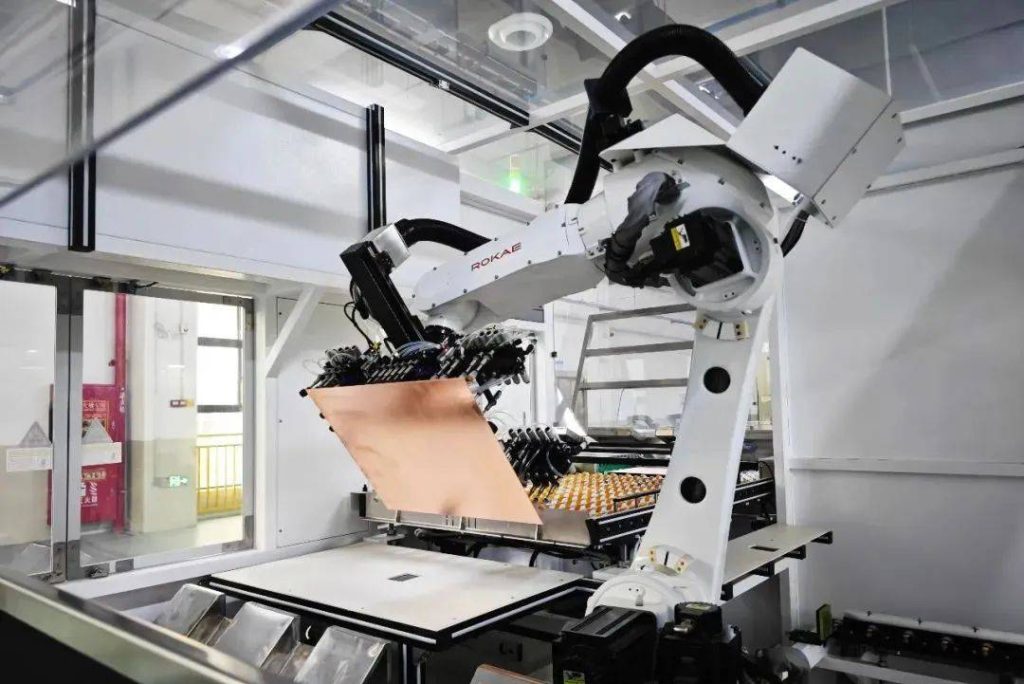
What is pcb layout? PCB layout, or printed circuit board layout, refers to the process of arranging all components, signal traces, ground planes, and power paths on a PCB board according to design specifications during PCB design. PCB layout is a crucial step in electronic design, as it directly impacts circuit performance, reliability, and manufacturing costs.
PCB Layout Process
Creating a PCB layout is by no means a simple operation; rather, it is a complex process encompassing multiple steps that requires careful planning and execution. The starting point lies in drawing the schematic diagram, which is a symbolic representation of the circuit, encompassing all components and their interconnections. The schematic diagram serves as the navigation chart for the PCB layout, while the PCB layout is the physical embodiment of the circuit.
Upon completing the schematic, the next step involves translating it into an actual PCB layout. This conversion process encompasses several critical stages, such as determining the precise placement of components on the board, planning the interconnections between them, and ensuring the entire design strictly adheres to industry standards and guidelines. Throughout this process, designers must comprehensively consider multiple factors, including the circuit’s electrical requirements, the physical constraints of the printed circuit board, and the manufacturing process.
Schematic Capture: The Cornerstone of Circuit Design
Schematic capture represents a pivotal stage in electronic circuit design, embodying the artistry of creating schematics – the blueprint for the entire circuit. This diagram comprehensively details all components alongside their complete schematic symbols, which are essential for understanding the electrical functionality and interconnections of each part. Today, specialised software greatly facilitates this process, enabling designers to seamlessly insert and arrange components while precisely drawing critical interconnections.
Schematic capture demands a deep understanding of circuit functionality. Designers must grasp each component’s role within the circuit, its interactions with others, and its contribution to the overall circuit performance. For instance, resistors may be employed to limit current flow within specific components to safe levels, while capacitors can be used to filter noise from the power supply.
From Schematic to PCB Layout: The Transformation into Physical Design
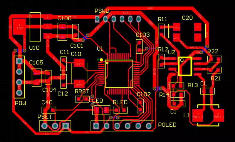
Once schematic capture is complete, it serves as the blueprint for creating the PCB layout. The layout process is the critical step in translating the schematic into a physical design, involving the precise positioning of each component on the board and the planning of interconnecting traces between them. This process requires designers to carefully balance electrical requirements, physical constraints, and design rules to ensure the printed circuit board is both functional and manufacturable. Component placement constitutes the core element of the PCB layout workflow, demanding designers’ meticulous attention to detail and strict adherence to design rules and guidelines. The objective is to create a layout that optimises electrical efficiency, minimises space utilisation, and complies with design rules, whilst coordinating the integration of surface-mount components, Allegro design software, and complex circuitry.
Component Placement: Critical Decisions Subject to Multiple Constraints
Component placement on printed circuit boards is governed by multiple constraints, each impacting the overall performance and reliability of the final product.
Electrical Considerations: Designers must group components with shared functions or signal paths logically, minimising interconnect lengths. This effectively mitigates signal attenuation and electromagnetic interference (EMI), safeguarding circuit integrity.
Thermal Management as a Core Priority: Thermal management is paramount in component placement. Components such as power transistors and voltage regulators generate significant heat and must therefore be positioned in areas with adequate airflow or proximity to heat sinks. This ensures efficient thermal dissipation, prevents overheating, and maintains equipment reliability.
Physical Constraints: The physical limitations of the printed circuit board and the components themselves are also vital considerations for placement. Components requiring substantial space or specific mounting hardware may necessitate placement in designated areas on the board. Additionally, components requiring maintenance or adjustment, such as connectors or potentiometers, should be placed in easily accessible locations.
Design Rule Compliance: Design rules and guidelines are typically dictated by industry standards or device-specific parameters. These rules cover aspects such as minimum spacing between components, clearances from the board edges, and alignment with other components. Strict adherence to these rules ensures the creation of a manufacturable PCB that meets industry standards.
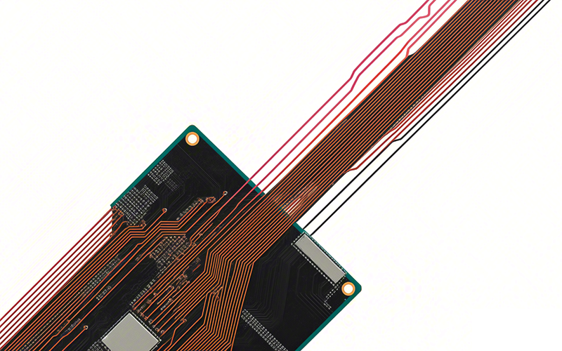
Routing: The Critical Path for Component Connectivity
Routing involves connecting components on a PCB via traces, typically made of copper, which provide pathways for current flow between components. This is a crucial aspect of PCB layout design, directly impacting circuit performance and reliability.
Adherence to design rules: When routing a PCB board, designers must ensure that the routing complies with design rules and guidelines, including minimum line widths, line spacing, and clearances from the board edges, to guarantee reliable and efficient PCB manufacturing.
Ensuring signal integrity: Signal integrity is a critical consideration during the routing phase, particularly in high-performance electronic circuit design. Designers must safeguard signal integrity as it traverses the PCB, minimising trace lengths and avoiding sharp bends (such as prohibiting 90-degree kinks), as these can cause signal attenuation and increase the risk of electromagnetic interference (EMI). Furthermore, high-speed signals and sensitive analogue signals should be routed away from noisy components like switching power supplies to reduce crosstalk risks and other signal integrity issues.
Optimising Power Distribution: Power distribution is another vital aspect of routing. Designers must ensure power traces are sufficiently wide to handle required currents and route them efficiently to minimise voltage drop. Ground planes—large copper areas connected to ground—provide low-impedance return paths for current, enhancing overall circuit performance.
Prioritising Thermal Management: Thermal management is a critical factor in PCB routing. Traces carrying high currents generate significant heat, potentially causing overheating and component failure. To mitigate this risk, designers may employ wider traces, incorporate heat sinks, or route components to maximise heat dissipation.
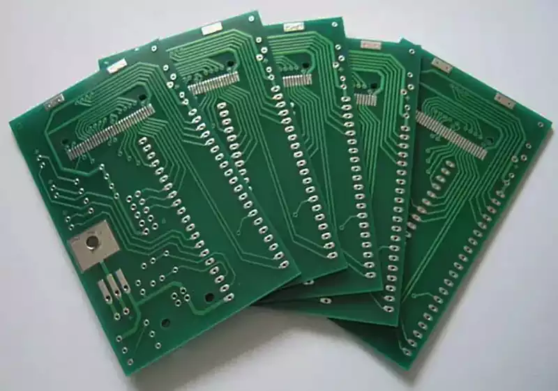
Component selection and circuit design constitute crucial benchmarks for evaluating an electronic product’s performance. Component placement and PCB layout, however, serve as vital stages for realising these characteristics. Each component and peripheral circuit design imposes specific layout requirements upon the PCB. Only through layouts adhering to these characteristic demands can product performance be effectively and efficiently realised.
Conventional PCB layout design processes encompass several fundamental steps, such as library component creation, net parameter configuration, component placement, signal routing, and design file output. However, this traditional design paradigm struggles to meet the demands of increasingly complex high-speed PCB design.
Today, SI simulation, PI simulation, EMC design, and single-board manufacturing processes are deeply integrated into the design workflow. Concurrently, review stages are added at critical junctures to enhance quality control, rendering the actual PCB layout design process significantly more intricate and meticulous.
PCB layout design has transcended mere electrical performance optimisation, evolving into a pivotal force that comprehensively shapes the circuit board’s exceptional electrical characteristics throughout product hardware development. A well-executed PCB layout design exerts a profound and fundamental influence on the board’s electrical performance. Through precise placement and routing operations, it efficiently minimises high-frequency signal transmission distances, substantially reducing signal delay and energy dissipation. Simultaneously, effectively mitigating electromagnetic interference (EMI) and signal crosstalk has become its core mission. Only by achieving this objective can the circuit board operate consistently and reliably in high-speed, high-density integration, and complex signal transmission scenarios, laying a solid foundation for the stability of the entire electronic system.
PCB layout design is no longer merely a supplementary activity loosely aligned with manufacturing processes; it has become a core element in ensuring the manufacturability of product hardware. It encompasses the precise and rational setting of critical parameters such as pad dimensions and interlayer via diameters. These parameters function like precision gears, directly determining the manufacturing quality of the circuit board. A scientifically sound design solution acts as a rigorous guardian, effectively preventing quality issues such as board warping and cold solder joints during production. This significantly enhances the finished product’s yield rate and operational reliability, establishing a robust defence for the hardware’s manufacturability.
PCB layout design has evolved beyond a tool for crude balancing of cost and efficiency. It now serves as a vital driver for achieving fine-tuned coordination and synergistic optimisation of cost and efficiency within hardware development. Through deep optimisation of PCB layout design, it becomes possible to streamline the number of circuit board layers, reduce the quantity of vias, and rationally plan component placement. These optimisation measures function like a precision scalpel, offering substantial benefits in reducing material costs and assembly complexity. Moreover, meticulously optimised designs substantially enhance production efficiency, effectively shortening manufacturing cycles. This, in turn, further reduces overall production costs, achieving balanced development of cost and efficiency. It provides robust support for maximising the economic benefits of product hardware.
GEOPCB, as a PCB layout and one-stop service provider, possesses a professional design team to undertake schematic design, PCB layout and simulation optimisation, offering DFM recommendations to ensure design feasibility. Utilising advanced manufacturing processes, it completes material selection, lamination and other production stages to deliver compliant circuit boards under stringent quality control. Comprehensive testing and an established quality traceability chain guarantee product stability and reliability. The company supports small-batch trial production, rapid response to design changes, and provides customised solutions. Additionally, our dedicated technical support team delivers comprehensive after-sales service, promptly resolving customer issues to enhance satisfaction.