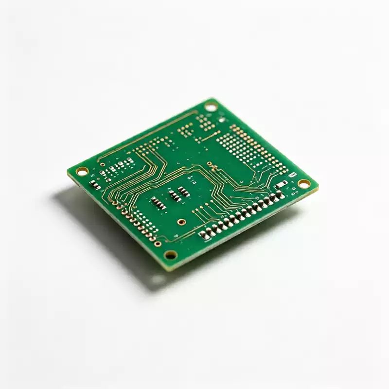
PCB manufacturing cost is one of the most persistent points of confusion for hardware teams. Two boards that look almost identical on screen can differ several times over in price, and two quotes against the same files can disagree because each fab is pricing a different manufacturing reality. Once you understand what actually drives pcb manufacturing cost, quoting stops being a guessing game and becomes an engineering decision you can influence.
This guide breaks down the real cost drivers, explains where the money goes, and shows which specification choices move the price the most.
Why PCB pricing has no standard price list
Unlike components with published distributor pricing, every PCB board order is a custom fabrication run. A fab prices your board by the panel area it occupies, the processes that panel must pass through, and the yield risk it carries. Change any of those and the price changes, even when the board outline stays identical.
That is also why per-board pricing falls as quantity rises: setup, tooling, and testing costs are spread across more units, and larger orders use panel area more efficiently. A ten-piece prototype and a ten-thousand-piece production run are not the same product priced at different volumes; they are genuinely different manufacturing economics.
The main cost drivers in PCB manufacturing
The drivers cluster into three groups, depending on where the decision actually gets made. Some are locked in at the CAD station long before a fab ever sees the files. Some are chosen when the board reaches the production floor. And some are made at purchase time, by people who never touch the design at all.
Choices made in design
Layer count is usually the single largest price lever. Each added layer multiplies the number of lamination, drilling, plating, and imaging cycles a panel must survive, and every cycle adds material, process time, and yield risk. A four-layer board typically costs noticeably more than twice a two-layer board for exactly this reason: cost scales with process steps, not with copper area. The stackup itself, not just the layer count, sets how difficult the build becomes.
Material sets the baseline. Standard FR4 is the economical default for most designs, while high-Tg grades cost more but tolerate higher assembly and rework temperatures. High-frequency materials such as Rogers laminates carry a significant premium because they are formulated for controlled dielectric performance rather than for price. The same logic applies within a family: a mid-tier FR4 grade usually meets the requirement that a designer assumed only a premium laminate could meet.
Copper weight behaves similarly. Heavier copper demands longer plating time and tighter etching control, and fine traces with tight tolerances shrink the process window the fab can run in. Every tolerance tightened removes process latitude, which raises both unit cost and scrap risk. One-ounce copper with sensible trace widths is the workhorse; two-ounce copper and beyond should be a deliberate current-carrying or thermal decision, not a default.
What this looks like in practice: a four-layer board on standard FR4, one-ounce copper, and a conventional finish sits at the economical end of the spectrum. The same board specified on a high-frequency laminate with two-ounce copper and Class 3 testing moves into a different price bracket entirely. No single choice in that sentence is exotic. The price moves because each one adds process steps.
Choices made in fabrication
Hole structure is where density starts to cost money. High-density designs push hole counts up and hole sizes down, and blind vias, buried vias, microvias, and HDI stackups require sequential lamination cycles and specialized drilling. That is why HDI boards price above conventional multilayer boards with the same layer count. If the density can be achieved with through-hole vias and a reasonable hole size, the saving is real.
Surface finish is a smaller lever, but an instructive one. ENIG, HASL, immersion tin, and OSP are different processes with different costs. ENIG costs more than HASL but delivers the flat pads that fine-pitch components need; OSP is the least expensive option and the least forgiving across multiple reflow cycles. Specifying ENIG on a coarse-pitch board is a recurring example of paying for margin nobody uses.
Then there is panel utilization, the quietest driver on the list. Fabs buy process capacity in panels. A board size that nests with little wasted edge is cheaper per unit area than an awkward size, and very small boards are usually cheaper as panelized arrays broken apart after assembly. Standard sizes and sensible clearances reduce every downstream cost at once.
Choices made at order time
Testing is specified by people who will never touch the design, and it is often the last place anyone looks for savings. Electrical testing, whether by flying probe or fixture, adds cost per board but catches opens and shorts before they become field failures. IPC Class 3 work demands more inspection, documentation, and process control than Class 2. Neither is wrong; the mistake is paying for Class 3 assurance on a product that does not need it, or paying for no testing at all on one that does. What electrical testing catches at this stage is far cheaper to fix than anything found after assembly.
Lead time rounds out the list. Rush orders compress the queue and usually carry a premium, because expedited work displaces production that was already batched and scheduled. A standard lead time is one of the easiest cost concessions available to a team that plans ahead.
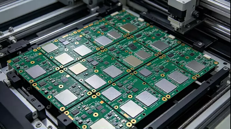
Where the money actually goes
The table below summarizes how each driver typically behaves. The direction of impact is consistent across the industry; the magnitude depends on the fab, the design, and the order.
| Cost driver | Typical impact | What you control |
|---|---|---|
| Layer count | Very high | Consolidate routing, avoid speculative layers |
| Material choice | Medium to high | Specify the cheapest grade that meets the requirement |
| Copper weight | Medium | Match weight to current and thermal needs |
| Via structure | Medium to high | Use through-hole vias where density allows |
| Surface finish | Low to medium | Match finish to assembly process |
| Panel utilization | Low to medium | Prefer standard sizes and panelization |
| Testing and class | Medium | Choose the test coverage the product justifies |
| Lead time | Low to medium | Plan orders against a standard queue |
How to reduce PCB manufacturing cost without sacrificing reliability
The goal is never to make a worse board. It is to stop paying for capability the design does not use. Five levers do most of the work.
- Right-size the layer count. Four layers that meet the requirement beat six that do not need to exist.
- Default to standard materials and finishes, and escalate only when a measured requirement, not a habit, demands it.
- Design for manufacturability from the start. A design that respects process limits avoids the respin, and a respin is the most expensive event in any PCB board program.
- Relax tolerances that do not matter. Tight is not free; every tightened tolerance is paid for twice, in unit price and in scrap.
- Buy in quantities that match the panel. One consolidated order beats three rushed small ones on both price and schedule, and the testing level should follow the product’s failure cost rather than a default.
What to include when requesting a PCB manufacturing quote
Quote quality depends on package quality. A complete request includes Gerber files, the stackup drawing, material and finish specifications, quantity, testing class, and delivery requirements. A complete package earns an accurate price; an incomplete one earns a padded one, because the fab prices the ambiguity. Teams that put together a disciplined custom PCB request consistently get tighter numbers and fewer surprises.
Frequently asked questions
Why does a four-layer PCB cost more than twice a two-layer board?
Because pricing follows process cycles rather than board area. A four-layer board passes through additional lamination, drilling, and plating steps, and each step carries its own material, time, and yield risk. The relationship between layer count and price is closer to multiplicative than additive.
Is the cheapest quote always the best value?
Not necessarily. A low quote often assumes thinner material, less testing, looser inspection, or a longer queue than your program can absorb. Compare quotes specification by specification, because two prices only mean the same thing when the boards behind them are identical.
Does a faster lead time always cost more?
Usually, yes. Rush work displaces batched production and forces the fab to re-plan its queue, and that disruption is priced into the order. When schedule allows it, a standard lead time is the single easiest cost concession available.
PCB manufacturing cost is not a mystery tariff. It is the sum of process steps your design demands, and almost every one of those steps traces back to a choice made at the CAD station. Layer count, material, via structure, finish, testing, and schedule each carry a visible price, and each can be specified with intent. Teams that treat pcb manufacturing cost as a design parameter rather than an afterthought get better boards at better prices, and they stop being surprised by quotes.