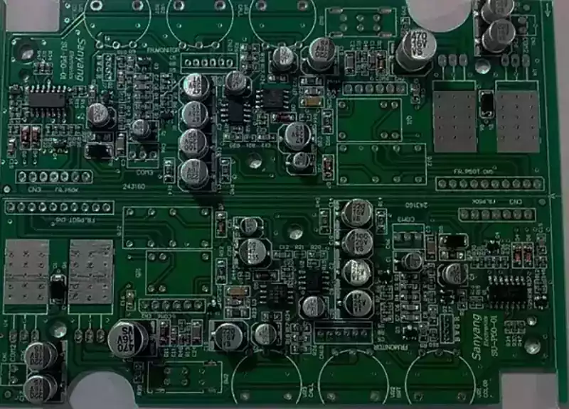
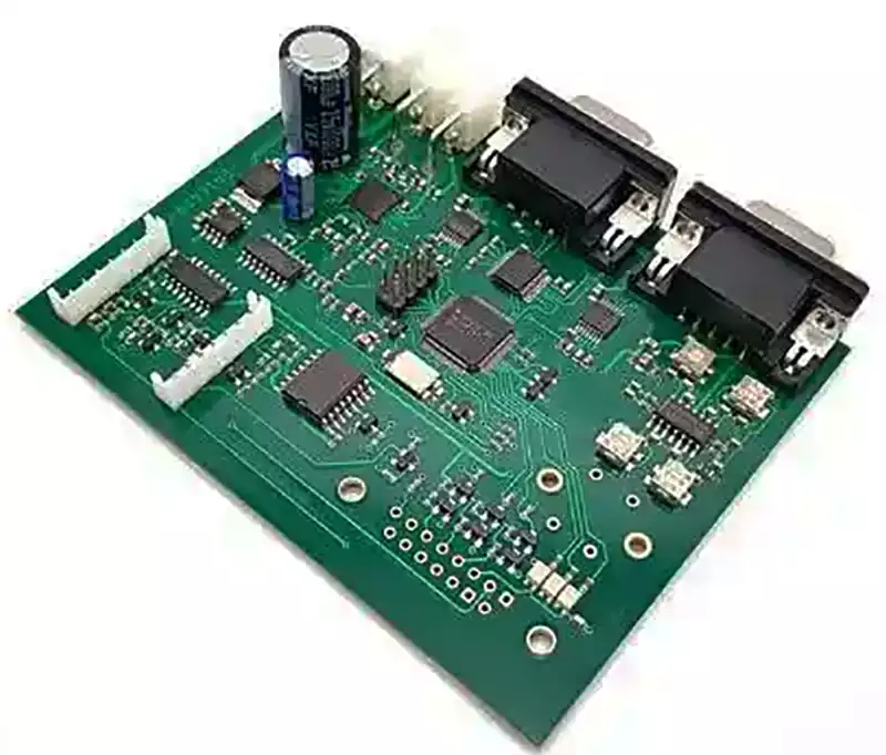
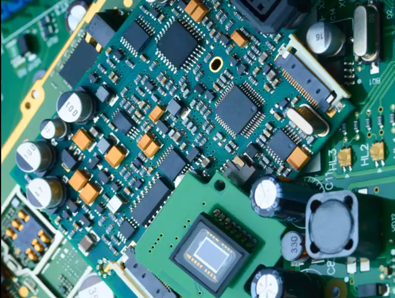
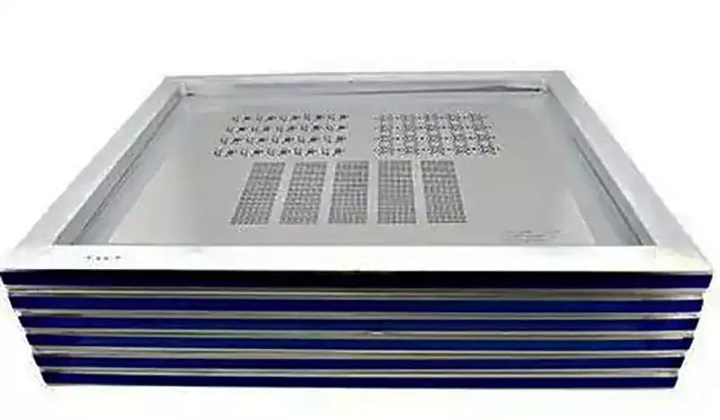
PCB stencils, also known as SMT stencils, SMT templates, or SMT stencils, constitute an indispensable component of the SMT (Surface Mount Technology) process. Their core function lies in precisely dispensing solder paste or red glue onto the pads of a PCB through their apertures, thereby establishing a robust foundation for the placement and soldering of electronic components.
Within PCB manufacturing, pcb stencils are primarily employed in the placement process, serving to apply solder paste to the pads of surface-mount packages during soldering. By featuring apertures precisely aligned with the placement pads, the stencil enables solder paste to flow accurately into the pads, thereby achieving precise soldering. Consequently, the stencil layer within EDA software exists solely for surface-mount devices, while through-hole components do not require this layer.
Common pcb stencil dimensions include: 37cm × 47cm, 42cm × 52cm, 55cm × 65cm, 60cm × 65cm, 65cm × 65cm, and 73.6cm × 73.6cm. Typically, fully automated solder paste printers used on SMT assembly production lines require a minimum stencil size of 42cm × 52cm.
Common pcb stencil types include: solder paste stencils, red glue stencils, stepped stencils, laser-cut stencils, and dual-process stencils. Stencil thickness specifications vary widely, with common options being 0.8mm, 1.0mm, 1.2mm, 0.13mm, 0.15mm, 0.18mm, 0.2mm, 0.25mm, and 0.3mm. Among these, solder paste stencils typically range from 0.05mm to 0.15mm in thickness, while red glue stencils generally measure between 0.18mm and 0.3mm.
Solder paste stencil:
Within SMT assembly facilities, solder paste stencils see extensive application. Their manufacturing process is not rigidly fixed but requires flexible adjustment of aperture dimensions to meet specific process requirements. For components requiring substantial solder paste volume, increasing stencil thickness is generally avoided. Instead, solutions involve enlarging the pad size and stencil aperture. This is because excessively thick solder paste stencils may cause processing issues such as short circuits in densely packed ICs and similar components.
Red Paste Stencils:
With the increasing miniaturisation of components, red paste stencils are gradually being phased out in SMT assembly production processes. Currently, they are only retained for boards containing high-power components and CHIP devices, such as power supply boards.
Stepped Stencils:
The design feature of stepped stencils is the formation of two or more distinct thicknesses on a single stencil. This design addresses varying solder volume requirements for different components and accommodates mixed-size electronic parts on a single circuit board while maintaining soldering quality. To achieve precise solder volume control through printing different paste thicknesses on the same stencil surface, stepped stencils (i.e., STEP-UP local thickening and STEP-DOWN local thinning) were developed.
Laser-cut stencils:
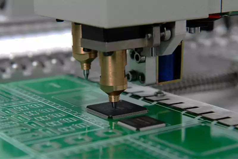
Laser-cut stencils are primarily manufactured by machine to transfer precise quantities of solder paste or red solder paste to designated positions on bare PCBs. Operators need only design apertures and import/export files; laser cutting machines then engrave the stencils according to these specifications. Subsequent polishing enhances solder deposition performance, delivering both rapid production and superior quality.
The Critical Role of PCB Stencils in SMT Assembly
Precise Solder Paste Application: Stencils control the quantity and placement of solder paste through their aperture size and arrangement, ensuring each pad receives the correct amount. High-precision stencils guarantee accurate paste printing at pad centres, reducing alignment challenges during placement and enhancing placement accuracy and efficiency. Conversely, poorly crafted stencils or ill-designed apertures cause paste misalignment or uneven distribution, potentially leading to soldering defects.
Enhanced Production Efficiency: In SMT assembly, time equates to money. The utilisation of stencils substantially boosts production efficiency. Through precise stencils and positioning techniques, the SMT process ensures components are accurately placed onto designated PCB board locations, thereby shortening production cycles. Furthermore, SMT reusable stencils enable swift installation and replacement of active stencils, further elevating production efficiency.
Reduced Product Costs: Beyond boosting efficiency, stencil usage contributes to lower production expenses. SMT reusable stencils employ reusable frames, offering greater cost-effectiveness than traditional disposable aluminium frames. Moreover, the high placement speed of SMT processes reduces manual intervention, thereby cutting labour costs.
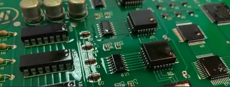
Ensuring Soldering Quality: Soldering quality directly impacts the reliability and lifespan of PCBA products. As the critical tool for solder paste printing, the stencil’s quality and condition directly influence soldering outcomes. On one hand, stencil cleanliness and flatness affect solder paste printing results, thereby influencing wettability and bonding strength during soldering. On the other hand, stencil wear and deformation can degrade printing quality, increasing the risk of soldering defects.
Selecting the Appropriate PCB Stencil
Choosing the right pcb stencil is crucial for ensuring SMT assembly quality. When selecting a stencil, the following factors must be considered:
Material Selection: PCB stencils are typically crafted from stainless steel or other alloy materials. Different materials exhibit varying degrees of hardness, corrosion resistance, and wear resistance. Therefore, the choice of material should be tailored to the specific application scenario and frequency of use.
Thickness and Aperture Size: The thickness of the PCB stencil and the size of its apertures directly influence the solder paste printing effect. Generally, thinner stencils with smaller apertures deliver finer printing results but may increase the risk of clogging. A balance must therefore be struck between printing precision and operational stability.
Manufacturing Process: Different production methods affect the stencil’s accuracy and durability. Laser cutting and electrochemical etching are two common techniques, each with distinct advantages and disadvantages requiring selection based on specific requirements.
Maintenance and Care: Screens require regular cleaning and upkeep during operation to remove clogged solder paste and contaminants, ensuring optimal performance. Selecting appropriate cleaning agents and maintenance methods is crucial for long-term, stable screen usage.
The selection and application of PCB stencils demand careful consideration. Comprehensive evaluation of multiple factors coupled with diligent maintenance are essential to guarantee the smooth execution of SMT assembly processes and uphold product quality.