What is PCB? PCB meaning Printed Circuit Board, also known as a printed wiring board. It refers to a printed board formed on a common substrate according to a predetermined design, featuring interconnections between points and printed components. Serving as the support structure for electronic components, it acts as the carrier for their electrical interconnection.
As a critical component within electronic products, the PCB plays an indispensable role. It not only shoulders the crucial task of circuit connection but also provides robust support for electronic components. More significantly, PCB circuit boards enhance circuit stability and reliability, ensuring electronic devices operate consistently and efficiently. Consequently, within modern electronic technology, PCB boards are undeniably indispensable.
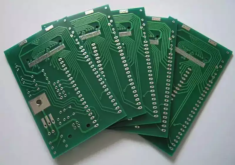
Printed circuit boards are primarily composed of insulating materials, such as fibreglass-reinforced epoxy (FR-4). They incorporate one or more thin copper layers, upon which circuit patterns are formed through chemical etching or mechanical machining. Electrical connections between copper layers are achieved via through-holes (via holes) or blind vias (connecting only between certain layers). Through the combination of wiring and insulating materials, the PCB circuit board enables electrical connections and functional integration of electronic components. It not only significantly enhances the integration and reliability of equipment but also saves wiring space and simplifies system design.
Compared to the earlier ‘wire-bonding’ method, the advantages of PCB boards lie in their integration, standardisation, and miniaturisation, manifested in three key aspects:
Superior electrical stability: Copper foil traces are precisely etched by machinery, ensuring uniform line widths and spacing. This eliminates the risks of poor contact and short circuits inherent in manual wiring, resulting in more stable signal transmission (particularly for high-frequency signals);
Enhanced space utilisation: Designs can incorporate single, double, or multiple layers (e.g., 4-layer, 6-layer, 12-layer), with components mounted on both sides of the board (via SMT processes), substantially reducing equipment footprint (e.g., mobile phone motherboards, laptop motherboards);
Low mass production costs: Standardised production processes (design → board fabrication → soldering) enable batch replication, making it suitable for large-scale electronic device manufacturing. During repairs, ‘silkscreen markings’ (e.g., R1, C2, U1) facilitate rapid component identification.
Composition of PCB board
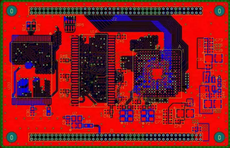
(1) Wire: The wire (Track) has a network connection relationship corresponding to the schematic diagram, and the wire has a network label (NetLable) corresponding to the circuit diagram nodes. When wiring, wires can be automatically pushed, wrapped, etc. (wires are connected through nodes, where there are no nodes, physical cross connections of wires are not allowed during wiring).
(2) Copper laying: Connect the network through a single piece of copper foil, and after wiring is completed, fill the remaining part of the PWB board with copper foil, usually used for ground (GND) and power (POWER). Due to the large area of copper foil, the heat dissipation effect will be more objective.
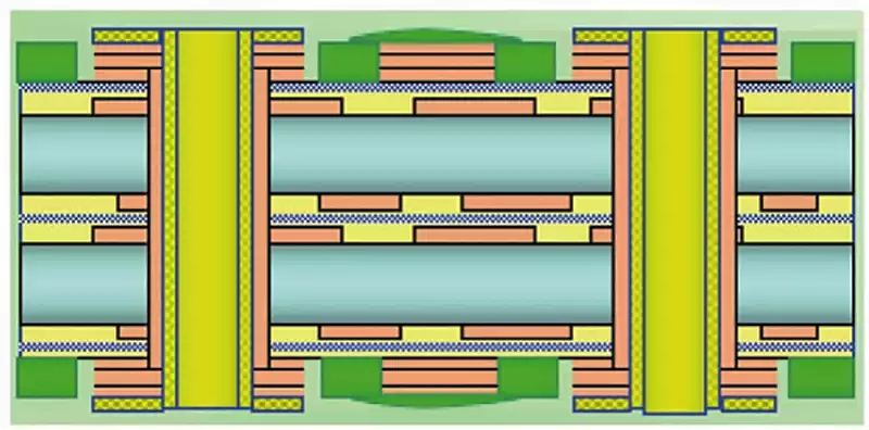
(3) Through hole:
① The function of vias:
Electrical connection: Through holes can be used to connect circuits at different levels, enabling effective signal and power transmission on the circuit board at different levels. Printed wiring board is generally divided into two layers, and with each additional layer, the cost increases dramatically
Device fixation or positioning: Through holes can be used to fix the position of electronic components such as resistors, capacitors, etc., ensuring their correct layout on the circuit board.
② Classification of through holes:
Through holes: The most common and simplest PWB board through holes are through holes, which are mechanical drilling holes drilled from the top to the bottom of the PCB.
Blind hole: Blind hole is a type of laser drilling that involves drilling and electroplating holes from the top or bottom layer of a pwb board to the inner layer.
Burial hole: Burial hole can be laser drilling or mechanical drilling, referring to the connection hole located in the inner layer of the printed circuit board, which does not extend to the surface of the circuit board.
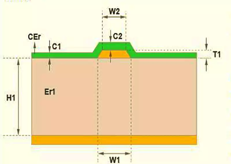
(4) Solder pads: Components are fixed to the PCB board by soldering through lead holes on the printed wiring board. Printed wires connect the solder pads to achieve electrical connection of the components in the circuit. The lead holes and the surrounding copper foil are called solderpads.
(5) Silkscreen: Silkscreen refers to the information printed on electronic circuit boards, such as text, logos, graphics, etc. These screen prints have important functions, they can help identify the position, value, model and other information of electronic components, as well as the direction and correct installation method of components.
Application Scenarios of PCB Boards
Communication Equipment: PCB boards are utilised in telephones, mobile phones, radios, satellite communication systems, and similar devices, providing reliable signal transmission pathways to ensure accurate data transfer.
Medical equipment: PCB boards are employed in diagnostic and monitoring devices, surgical instruments, and implantable devices, meeting stringent precision and reliability requirements to safeguard equipment functionality and patient safety.
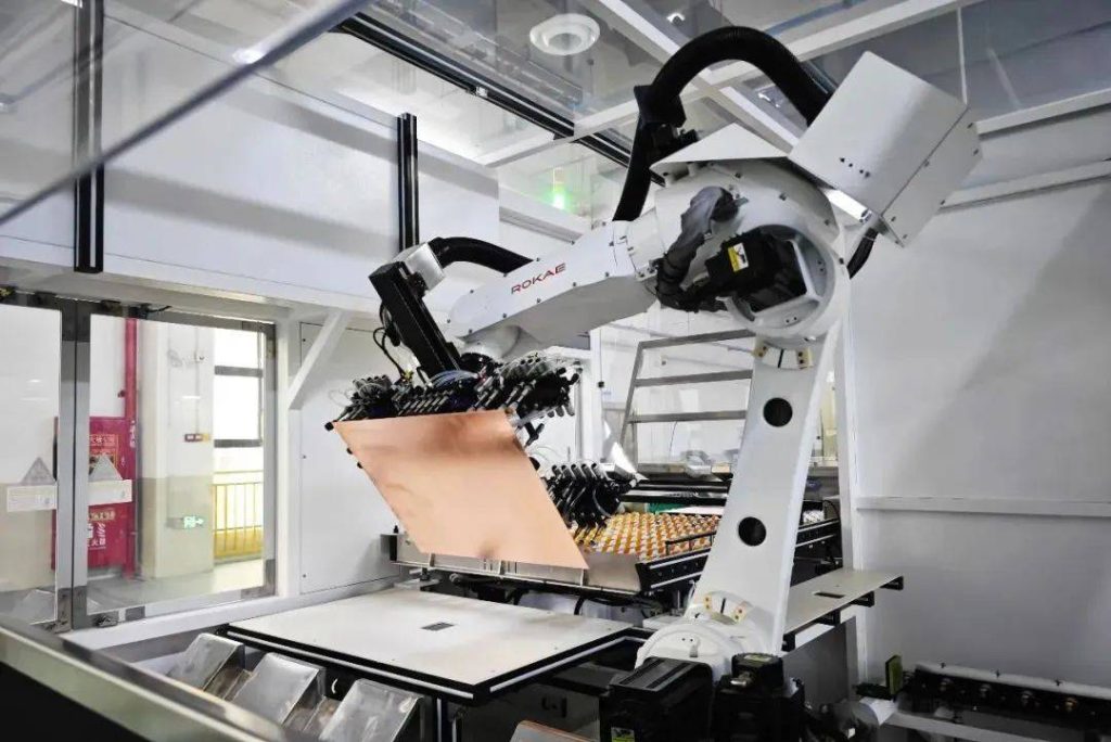
Industrial control: PCB circuit boards are utilised in robotics, CNC machine tools, and production line automation systems, enabling precise control and operation.
Automotive Electronics: Printed circuit boards (PCBs) are employed in engine control modules, body control modules, and airbag control systems, managing various vehicle systems to ensure proper functioning.
Consumer Electronics: Printed circuit boards (PCBs) are utilised in household appliances such as televisions, refrigerators, washing machines, and air conditioners, as well as in smartphones, tablets, and video game consoles, providing electrical connections and component support.
Aerospace: Printed circuit boards (PCBs) are utilised in aircraft, rockets, and satellites, meeting stringent reliability and precision requirements to execute complex control and monitoring functions.
Computers and Servers: PCB circuit boards are employed in computers and servers, providing dependable signal transmission pathways to ensure rapid data transfer and processing.
Internet of Things (IoT) Devices: PCB circuit boards furnish stable, reliable control and data transmission pathways for IoT devices, enabling intelligent management and remote monitoring.
New Energy Sector: PCB circuit boards are employed in solar panel systems, wind power generation systems, and similar applications, delivering electrical connections and control functionality.
Classification of Printed Circuit Boards
Printed circuit boards are categorised by the number of layers into three main types: single-sided circuit boards, double-sided circuit boards, and multilayer pcb boards.
Single-sided circuit boards feature components concentrated on one side of the most basic PCB, with conductive traces concentrated on the opposite side. As traces appear on only one side, this type of PCB is termed a single-sided circuit board. Single-sided boards are typically simple to manufacture and cost-effective, though their disadvantage lies in their inability to accommodate overly complex products.
Double-sided circuit boards represent an extension of single-sided boards. When single-layer routing fails to meet electronic product requirements, double-sided boards are employed. Both sides feature copper cladding and traces, with vias connecting circuits between layers to form the necessary network connections.
Multilayer pcb boards refer to printed circuit boards comprising three or more conductive pattern layers laminated together with insulating materials between them, where the conductive patterns are interconnected as required. Multilayer circuit boards represent the evolution of electronic information technology towards high speed, multifunctionality, large capacity, compact size, thin profiles, and lightweight designs.
Multilayer pcb boards are commonly designated by even numbers, such as 2, 4, 6, 8, 10, 20, 40, or 100 layers. Simply put, the number of copper layers—i.e., the number of traces—equates to the board’s layer count. Presently, most multilayer processes involve laminating multiple double-sided copper-clad laminates, hence the prevalence of even-numbered multilayer boards. For instance, laminating two double-sided pcb boards yields a 4-layer board; adding one more double-sided circuit board results in a 6-layer board, and so forth. Furthermore, advanced technologies like HDI, SLP, and Anylayer, despite their complexity—characterised by numerous vias, fine traces, intricate processes, and high precision—still fall under the material category of ‘rigid boards.’ Thus, they are generally classified as multilayer boards unless specifically listed separately.
By Material Properties
Classification by Substrate Rigidity
Rigid PCB
Definition: Utilising rigid insulating materials as the substrate, incapable of bending or folding, representing the most prevalent type in electronic devices.
Representative Materials: FR-4 fibreglass cloth substrates, phenolic paper substrates, metal-clad laminates (aluminium-based, copper-based), etc.
Applications: Computer motherboards, smartphone mainboards, automotive electronic control modules, etc.
Flexible PCB Board
Definition: Utilising flexible materials such as polyimide (PI) as the substrate, capable of bending and folding to accommodate installation in confined spaces.
Representative Materials: PI substrates, polyester film substrates.
Application Scenarios: Wearable devices, hinge flex cables for foldable smartphones, minimally invasive medical surgical instruments, etc.
Classified by Reinforcement Material
Glass Cloth Base
Core Components: Glass fibre cloth + epoxy resin (e.g., FR-4), offering high strength and heat resistance.
Advantages: Superior mechanical strength, stable dielectric properties, and excellent moisture resistance.
Paper-based
Core components: Wood pulp fibre paper + phenolic resin (e.g., FR-1, XPC). Low cost but limited performance.
Limitations: Poor temperature resistance (typically <130°C), suitable only for low-power devices.
Composite Base
Core components: Glass fibre cloth laminated with paper (e.g., CEM-1), balancing cost and performance.
Applications: Control boards for small appliances, electronic modules in toys, etc.
Classified by Specialised Function
Metal-based PCBs
Aluminium-based: Exceptional thermal conductivity, suitable for LED lighting and power amplifiers.
Copper-based: Thermal efficiency exceeds aluminium-based by over threefold, used in high-frequency communication equipment.
High-Frequency PCB
PTFE (Polytetrafluoroethylene): Low dielectric constant (ε=2.0-2.5), minimal loss tangent (tanδ<0.002), suitable for 5G base stations and radar systems.
Rogers Series: Offers stable high-frequency performance with dielectric constant precision up to ±0.02, making it the preferred choice for high-end RF circuits.
Ceramic-based PCBs
Aluminium Oxide (Al₂O₃), Aluminium Nitride (AlN): Resistant to high temperatures (>1000°C) with exceptional insulation properties, used in aerospace and high-power semiconductor modules.
Classified by via type: through-hole, blind via, buried via.
Through-hole: The hole penetrates the entire board, with both ends terminating on the top or bottom layer (the outermost two layers).
Blind via: One end of the hole terminates at the surface layer (outer layer), while the other ends at an inner layer without penetrating the entire board.
Buried via: Both ends of the hole are located within the board, connecting only two internal layers.
Factors influencing PCB circuit board pricing:
1.PCB circuit board costs vary significantly due to differing material selections. Taking a common double-sided board as an example, the substrate typically comprises FR4 types (including Shengyi, Jiantou, and Guojie brands, with prices decreasing in that order). Board thickness ranges from 0.2mm to 3.0mm, while copper thickness varies from 0.5oz to 3oz. The substrate alone thus accounts for significant price differences. Regarding solder mask ink selection, there is also a price differential between standard thermosetting ink and photosensitive green ink.
2.Variations in PCB surface finishing processes further contribute to price diversity. Common treatments include: OSP (Oxygen-Stabilised Phosphor), leaded hot-dip tin plating, lead-free hot-dip tin plating (environmentally compliant), gold plating, electroless gold plating, and various combination processes. These processes generally increase in cost sequentially.
3.The complexity of PCB design likewise impacts pricing. For instance, two boards each featuring 1000 holes may incur different drilling costs if one board’s hole diameter exceeds 0.2mm while the other’s is below 0.2mm. Similarly, if both boards share identical specifications except for trace width and spacing—one exceeding 4mil and the other below 4mil—this will generate differing production costs. Furthermore, designs employing non-standard manufacturing processes—such as half-plated through-holes, buried/blind vias, in-panel holes, or carbon ink printing on keypad boards—will incur additional charges.
4.PCB copper foil thickness also affects pricing. Common thicknesses include: 18μm (1/2oz), 35μm (1oz), 70μm (2oz), 105μm (3oz), and 140μm (4oz). Thicker copper foil commands higher prices.
5.PCB circuit board quality acceptance standards vary between clients, affecting pricing. Common standards include IPC2, IPC3, corporate specifications, and military standards. Higher standards correspond to increased costs.
6.Explanation of Tooling and Fixture Costs
Regarding tooling fees: For prototypes and small-batch production, PCB manufacturers typically employ drilling and milling for panel shaping, thereby avoiding additional edge-milling charges. However, large-scale production necessitates tooling for panel punching, incurring a tooling set cost.
7.Impact of Payment Methods on Pricing
Opting for payment methods with shorter settlement periods, such as cash payments, typically yields lower prices.
8.Impact of Order Quantity and Lead Time on Pricing
(1) Order Quantity: Smaller order volumes incur higher unit costs. Even for single-unit production, PCB manufacturers must complete all processes—including engineering documentation preparation and film output—resulting in higher per-unit cost allocation.
(2) Lead Time Requirements: Data submitted to the PCB manufacturer must be complete and accurate. This includes detailed specifications for Gerber files, number of layers, substrate type, pcb thickness, surface finish, ink colour, character colour, and any special requirements.