What is PCB design? PCB design refers to Printed Circuit Board Design. Circuit board design is based on circuit schematics to realise the functionality required by the circuit designer. PCB board design constitutes the physical framework construction process for electronic products, transforming abstract circuit diagrams into manufacturable physical board layouts that directly impact device performance, cost, and reliability.
PCB design primarily concerns layout design, necessitating consideration of external connection arrangements, optimised placement of internal electronic components, efficient routing of metal traces and vias, electromagnetic shielding, thermal dissipation, and various other factors. An excellent layout design can reduce production costs while achieving superior circuit performance and heat dissipation. Simple layouts may be achieved manually, whereas complex designs require Computer-Aided Design (CAD) software.
The quality of a PCB directly determines the success or failure of an electronic product, making a sound PCB board design process paramount. Many engineers mistakenly believe PCB design involves merely arranging components and connecting their pins. This is a narrow perspective; a robust PCB design process commences during schematic design, encompassing decisions such as selecting appropriate solutions and suitable electronic components.
The process specifically encompasses: schematic design; schematic netlist export and import; mechanical drawing import; stackup design and editing; pre-simulation of Signal Integrity (SI)/Power Integrity (PI); PCB layout; import of design constraint rules; PCB routing; post-simulation of Signal Integrity (SI)/Power Integrity (PI)/Electromagnetic Compatibility (EMC)/Thermal analysis; Design for Manufacturability (DFM) checks; and generation of production files (Gerber). These tasks may be undertaken by a single engineer or collaboratively by multiple engineers. Naturally, the PCB design process varies for each product, with specific requirements dictating the workflow. Design for Manufacturability (DFM) checks. Production file generation (Gerber). These tasks may be completed by a single engineer or collaboratively by multiple engineers. Naturally, not every product’s PCB design process is identical; specific products may refine, augment, or reduce this workflow as appropriate.
Widely used PCB design software includes:Altium Designer, offering comprehensive functionality from schematic design to PCB layout, package generation, and signal integrity analysis. Its visual environment and extensive tool library facilitate efficient design;
Cadence Allegro, a professional-grade tool widely adopted in industry, supports high-speed digital signal and RF circuit design with robust simulation and multi-user collaboration capabilities; Mentor PADS suits small-to-medium scale designs, covering the entire design workflow with a user-friendly interface; KiCad, an open-source solution, supports multiple platforms with robust functionality and an active community offering free technical support; Eagle is characterised by ease of use and rapid learning, featuring an intuitive interface and a large user community enabling design resource sharing.
Information Required for PCB Design
- Circuit Schematic Diagram
The schematic diagram forms the foundation of PCB board design, detailing all electronic components and their interconnections. Designers must base PCB layout and routing on this schematic. - Bill of Materials (BOM)
The BOM lists all components to be mounted on the PCB board, including part numbers, specifications, package types, and quantities. This aids designers in selecting appropriate component packages and layout planning. - Design Specifications and Requirements
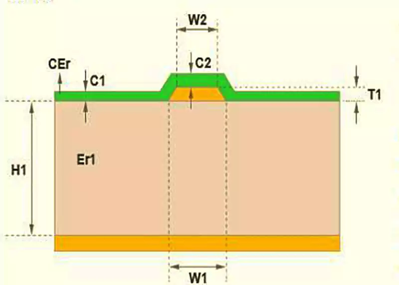
These encompass PCB dimensions, layer count, material, thickness, electrical performance requirements (e.g., impedance control), special process requirements (e.g., blind/buried vias, HDI), and other design constraints. - Reference Design Materials
Where available, similar reference design materials—such as prior project files or reference design drawings—should be provided to designers for consultation. - Mechanical Structure Drawings
Include outline drawings, mounting hole positions and dimensions, connector locations, and other mechanical structural information to ensure the PCB design aligns with the product’s overall mechanical requirements. - Testing and Debugging Requirements
Provide specific requirements for product testing and debugging, such as test point locations and test interfaces, enabling designers to appropriately arrange test points and interfaces within the PCB layout.
PCB Circuit Board Design Steps
The standard PCB design workflow is: Preliminary Preparation → PCB Structural Design → PCB Layout → Routing → Routing Optimisation and Silk Screen → Network and DRC Checks with Structural Verification → Panelisation.
(1) Schematic Design: Schematic design primarily involves drafting the schematic using the schematic editor within circuit board design software.
(2) Generating the Netlist: The netlist is a report displaying the connection relationships between components within the circuit schematic. It serves as the bridge linking schematic design to PCB layout. By examining the netlist, connections between components can be swiftly identified, facilitating subsequent PCB design.
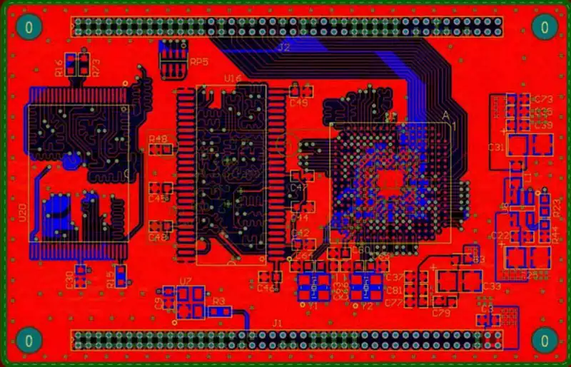
(3) PCB Board Design: PCB design implements required functionality based on the schematic diagram. Designing the PCB layout necessitates consideration of numerous factors, including mechanical structure, external connection layout, component placement, interconnections, thermal management, and electromagnetic compatibility. Completing this stage often requires numerous iterations of schematic revisions.
(4) PCBA Control Board Fabrication: Following component procurement and PCB receipt, the board undergoes SMT placement and soldering of various components, alongside DIP insertion processes, thereby completing the control board assembly.
Component Placement Principles
First, position components with close structural integration, such as power sockets, indicator lights, switches, connectors, and interfaces.
Second, place specialised components, including large components, heavy components, heat-generating components, and ICs.
Finally, position smaller components.
When arranging components, consider routing and prioritise layouts that facilitate wiring.
- Crystal oscillators should be positioned close to integrated circuits;
- Decoupling capacitors for integrated circuits should be placed as near as possible to the power pins of the IC, forming the shortest possible loop between power and ground;
- Heat-generating components should generally be distributed evenly to facilitate heat dissipation from the PCB and the entire unit. Temperature-sensitive components, except for temperature sensors, should be kept away from high-heat-generating components.
Routing Principles
- High-speed signal traces should be kept as short as possible, with critical signal traces minimised in length.
- Avoid placing too many vias on a single trace; limit to no more than two vias.
- Routing corners should preferably exceed 90 degrees; avoid angles below 90 degrees and minimise the use of 90-degree corners;
- When routing on double-sided boards, traces on both sides should be arranged perpendicular, diagonally, or curved to each other, avoiding parallel routing to reduce parasitic coupling;
- Audio input lines should be of equal length, placed close together with the audio line surrounded by a ground plane;
- No traces should run beneath the amplifier IC; multiple vias should be placed beneath the amplifier IC to connect to GND;
- As there is no ground plane layer in a double-sided board, the ground connection for the crystal oscillator capacitor should use the widest possible short trace to the GND pin closest to the crystal on the component, minimising the number of vias;
- Power supply lines and USB charging inputs shall employ thicker traces (≥1mm). Provide double-sided copper plating over via locations, then add multiple vias within the plated copper area.
Generally, power and ground traces should be routed first to ensure the PCB’s electrical performance. Where feasible, widen power and ground traces, ideally with ground traces exceeding power trace width. Trace priority is: ground > power > signal. Signal trace widths typically range from 0.2–0.3mm, with minimum widths of 0.05–0.07mm. Power traces generally measure 1.2–2.5mm.
Against the backdrop of accelerated evolution towards intelligent and highly integrated electronics, PCB design has evolved from a singular technical process into a pivotal hub connecting innovation with mass production. GeoPCB, with its comprehensive service chain spanning requirement analysis, schematic design, PCB layout routing, simulation verification, DFM manufacturability analysis, prototype production, and mass production support, GeoPCB delivers bespoke solutions for consumer electronics, automotive electronics, industrial control, and 5G communications sectors.