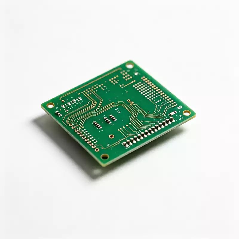
PCB thermal management is the discipline of giving the heat a chip or power device generates a reliable path out of the board, instead of letting it pile up near the junction. Most of that heat comes from the IC itself, power MOSFETs, LEDs, and power inductors. The board handles this by letting copper foil spread the heat sideways, pulling it through vias to an inner or backside plane, and adding heavy copper or a metal core to lift conductivity a notch.
Why PCB thermal management begins with base material conductivity
Heat moves sideways through copper foil and vertically through vias that pierce the insulating layers. The bottleneck is the substrate: FR-4 fiberglass epoxy has a through-plane conductivity of only 0.3 to 0.4 W/(m·K), while copper sits at 390 W/(m·K), a gap of nearly 1000x. A 1.6mm slab of FR-4 is, in effect, a layer of insulation.
The gap is easiest to see in a worked example. A 5×5mm pcb thermal pad dissipating 2W, if it relies solely on FR-4 to conduct inward, hits a temperature rise of 365°C by ΔT = P × L / (k × A). That is obviously unacceptable. Heat cannot move down through the substrate on its own; it has to spread sideways across the surface copper first, then travel through vias to an inner copper plane or a backside heatsink pad.
Two variables get underestimated more than they should. Copper weight is one of them: the same chip runs noticeably cooler on 2oz copper than on 1oz, simply because the cross-section available to spread heat is larger. The other is board thickness: a 1.0mm board gives thermal vias roughly 37.5% lower resistance than a 1.6mm board, because vertical conduction has less material to cross.
Thermal vias are the most common PCB thermal management tool
A thermal via is a row of plated holes placed directly under a heat source, carrying surface heat straight down to an inner or backside copper plane. The geometry is fairly settled by engineering consensus: a 0.3mm drill, spaced 1.0 to 1.2mm in an array. Under a 5×5mm QFN pad at 1.0mm pitch you can fit 25 vias.
Whether a thermal via works comes down to almost one thing: is there copper inside the hole. A 0.3mm drilled, 25µm-plated, 1.6mm-thick unfilled via sits at about 190°C/W; fill it with copper (IPC-4761 Type VII) and it drops to about 58°C/W, a 3.3x improvement per via. Array them and the effect compounds: 25 vias at 1.0mm pitch give about 6.7°C/W on a 1.6mm board or 4.2°C/W on a 1.0mm board; drop the density to 9 vias at 1.5mm pitch and resistance jumps back to 18.5°C/W.
Fill material splits into three classes with very different conductivity. Non-conductive epoxy (Type V) carries only 0.2 to 0.8 W/(m·K) and mainly stabilizes the structure and blocks solder wicking. Conductive epoxy (Type VI), loaded with silver or copper, reaches 1 to 10 W/(m·K). Copper fill (Type VII) lands at 390 W/(m·K) and pulls the resistance down hardest, but costs the most: it adds 15% to 25% to the base fab cost. A practical split goes like this: under 1W, epoxy fill is enough; 1 to 5W calls for conductive epoxy; above 5W, copper fill plus outer copper of 2oz or more.
Fill has a secondary benefit: an open via gets scavenged by solder during reflow, starving the pad and raising voiding, which disappears once the via is filled. On layout, the vias should fill the entire thermal pad area, stay at least 0.3mm from the pad edge to keep the solder mask web intact, and tie directly to a continuous inner plane, never through a thermal relief (spoke) connection.
The role of heavy copper in PCB thermal management
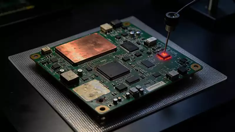
Copper weight drives both conduction and current carrying. 1oz is 35µm, 2oz is 70µm, and it goes up through 3oz (105µm) to 10oz (350µm). Thicker copper spreads heat over a larger area, lowering rise, and also raises ampacity.
Power boards and high-current modules commonly run 2oz to 4oz; very high power density pushes to 6oz or even 10oz, or buries heavy copper in inner layers. But thicker is not automatically better. Etch difficulty, z-axis height mismatch at lamination, yield, and unit price all climb with it. It is a tunable lever that has to be sized against current density and allowed rise, not added by guesswork.
When metal core boards become necessary for PCB thermal management
When power density gets high enough that FR-4 plus heavy copper struggles, the metal core board (IMS / MCPCB) enters. Its stack is three layers: a metal base (aluminum around 150 to 200, copper 380 to 400 W/(m·K)), a 50 to 150µm dielectric layer (1.5 to 4 W/(m·K), breakdown above 3000V), and a 1 to 4oz copper circuit layer on top.
Against FR-4, a metal core board cuts junction temperature by 20 to 40°C, lowers total resistance 40% to 60%, shrinks the same power supply by about 30%, and stays dimensionally stable through −40 to +150°C cycling, which suits automotive and outdoor vibration environments. LED light engines, headlamp modules, power inverters, and motor drives are its typical homes.
A tier up is the ceramic substrate: alumina at 20 to 30, aluminum nitride (AlN) up to 170 to 230 W/(m·K), with a coefficient of expansion close to silicon so almost no thermal stress forms. It is common in SiC/GaN power modules and traction converters. A localized option is the copper coin: a 0.5 to 3mm copper block pressed under a high-power device, cutting junction-to-case resistance 40% to 60%.
Metal core boards are limited by layer count; they cannot do the dozen-plus layers of an FR-4 high-density interconnect. So dense routing and strong cooling usually have to be planned separately: the interconnect goes to the FR-4 multilayer, the heavy cooling to metal or ceramic, rather than expecting one material to cover everything.
One PCB thermal management mistake can fail in the field
Thermal design errors show up directly in the field, and mostly after volume production. Miss any one of the methods above and it returns as a concrete failure.
The easiest place to lose is the thermal relief (spoke) connection: any via or inner layer tied through spokes adds 5 to 15°C/W of resistance per joint, so they must be fully connected instead. Too few vias is just as fatal. A single 0.3mm unfilled via is about 190°C/W; a 3W device with only a handful of vias sees a rise into the hundreds of degrees and typically needs 9 to 25 or more to stay controlled.
Open vias also get scavenged by solder in reflow, causing weak joints and voids. Forgetting backside copper coverage is another one: the backside copper area should be at least 4x the device’s thermal pad, or the heat simply has nowhere to go. And ignoring board thickness, running a 1.6mm board where a 1.0mm would have been far better, is a quiet mistake.
These failures are specific in the case record. Automotive ambient can reach 125°C, and under FR-4’s Tg (130 to 170°C) that leaves only about 25°C of rise margin, so miscalculating the thermal budget by a little crosses the line. An LED board on plain FR-4 without a metal core runs the junction past 125°C long term, and lumen decay, color shift, and life all drop sharply. In a power module, a MOSFET with thin copper and no thermal vias under it delaminates and opens after sustained full load. Past Tg, FR-4 softens, separates, and blisters, which is irreversible damage rather than a false alarm.
Engineers usually ask these questions about PCB thermal management
How many thermal vias are enough? There is no fixed number; it depends on device power, allowed rise, and copper weight. Set the junction ceiling and ambient, back out the allowable θJB, then calculate the via count and whether to fill. 9 to 25 is a common range, and dense designs need more.
How much cooler is 2oz versus 1oz copper? Doubling copper weight nearly doubles the spread capacity for the same cross-section, and rise drops clearly. The exact number still depends on layout, whether there is a heatsink plane, and via support, so copper weight alone does not decide it.
Can a metal core board replace heavy copper FR-4? They do not substitute for each other. Metal core conducts strongly but is layer-limited, suiting high power density with simple interconnect; FR-4 multilayer routes flexibly and leans on heavy copper and thermal vias for cooling. Which to pick comes down to whether device density or cooling demand is the tighter constraint.
PCB thermal management is best settled at the stack-up and package-selection stage. Take a power device and first pin down its junction ceiling, ambient ceiling, and remaining resistance margin, then work back to the copper area, via count, and whether heavy copper or a metal core is needed. Spending half a day on that math at the schematic stage beats recalling an entire batch after production.