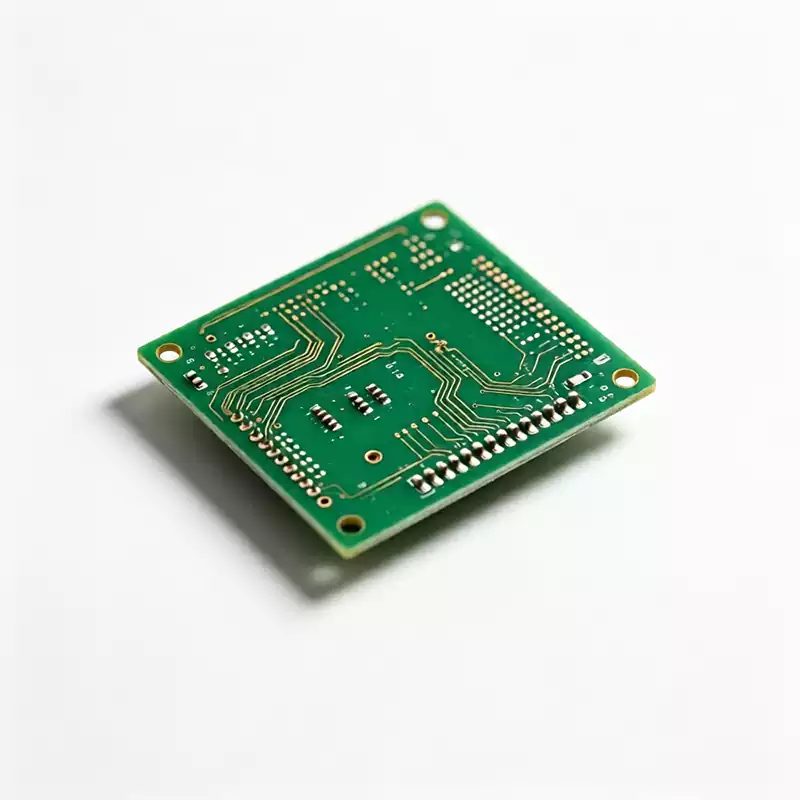
AI server PCBs are the most demanding circuit boards in volume production today. A traditional server runs 8 to 16 layers on standard materials; an AI training node runs 20 to 40 layers and beyond on laminates that cost three to ten times more per square meter, carrying signals at 224 Gbps and heading for 448 G. Nothing about that is a incremental upgrade. It is a different manufacturing category, and the gap between a fabricator who builds AI server PCBs and one who claims to is measured in certifications, equipment, and yield data.
What makes AI server PCBs different
Three things change when a server becomes an AI server: the architecture, the signal rate, and the power density.
The architecture shifts from CPU-centric to CPU plus GPU clusters. A traditional server board carries one processor and its memory. An AI training node carries multiple GPU modules, the circuit boards that connect them to each other, and the switch fabric behind them. NVIDIA’s DGX H100 generation added two new circuit board types to every server: OAM modules that carry individual GPUs, and a UBB baseboard that interconnects eight of them. The GB200 generation replaced that arrangement with large Superchip boards carrying CPU and GPU pairs together.
The signal rate is the harder problem. AI accelerators move data over SerDes channels that have moved from 112 Gbps to 224 Gbps per lane, with the next platform generation targeting 448 Gbps. At those rates, insertion loss budgets are measured in fractions of a decibel, and every via, every connector transition, and every centimeter of glass weave matters.
Power density completes the picture. An AI rack draws several times the power of a traditional rack, which means thick copper, dense power distribution, and thermal design that treats the board as a heat-spreading component rather than a passive carrier.
AI server PCB layer counts and where they are going
Layer count is the most visible symptom of the AI server PCB problem, and the trajectory is steep. NVIDIA’s own platform generations tell the story:
| Platform | Typical layer count | Laminate grade |
|---|---|---|
| DGX H100 (Hopper) | ~22 layers | M6 / Megtron 6, very low loss |
| GB200 (Blackwell) | ~22 layers | M7 / Megtron 7, ultra low loss |
| GB300 (Blackwell Ultra) | 22–34 layers | M7 / Megtron 7 |
| VR200 (Rubin) | 26 layers compute, up to 44 midplane | M8 with quartz glass |
| Rubin LPX | ~52 layers | M9 with quartz glass |
| Rubin Ultra (Kyber) | 78+ layers | M9+ quartz, M10 in qualification |
Compare that with a general-purpose server at 8 to 16 layers, and the direction is clear: AI server PCB stacks are heading toward 50 and 78 layers as platforms add GPU count and memory channels faster than they add board area.
The economics follow the layer count. Per-GPU PCB value rose from roughly $175 on DGX A100 to $211 on H100 to $346 on GB200 NVL72, and the rack-level bill of materials shows PCB content growing from about $35,100 on GB300 to $116,730 on VR200, a 233% increase in a single generation. Boards above 18 layers now sell at $1,500 per square meter and up, more than three times the price of mid-range multilayer product.
The materials behind AI server PCB performance
Layer count alone does not deliver signal integrity. The laminate does. AI server PCB programs specify copper-clad laminates by loss grade, and the grades are a steep staircase:
- M6 (very low loss) is the entry point, used for CPU boards and GPU modules on earlier generations
- M7 (ultra low loss) carries the high-speed interconnects on GB200 and GB300
- M8 and M9 are the current frontier, required for 224 Gbps channels and specified for the Rubin platform family
- Quartz glass fabric replaces standard E-glass at the top grades because its dielectric stability holds at high frequency
The target numbers explain the obsession. AI server PCB materials need dielectric constant at or below 4.0 and dissipation factor at or below 0.015, versus roughly 4.5 and 0.02 for high-end FR-4. The cost difference is brutal: an M9 laminate runs around 400 yuan per square meter, about ten times standard FR-4, with M7 at roughly three times and M8 at six and a half.
Two upstream materials gate the whole supply chain. HVLP copper foil, the extremely smooth foil these laminates require, is produced by only three suppliers worldwide who control 80 to 90% of usable capacity. Low-dielectric and quartz glass fabrics are concentrated among Japanese producers. A fabricator with lamination presses but no secured material pipeline does not have an AI server PCB capability, regardless of what the capability sheet says.
Why AI server PCB manufacturing is hard
The manufacturing gap is where most fabricators fail, and it shows up in four places.
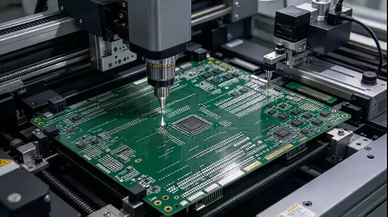
Registration and lamination. A 40-layer stack that drifts out of registration is scrap. Building boards above 30 layers means sequential lamination cycles, each one an opportunity for warp, delamination, and misregistration, with yields that fall with every added layer.
Via technology. High-aspect-ratio drilling, sometimes beyond 40 to 1, and hole diameters approaching 50 micrometers push mechanical drilling to its limits and force laser drilling and backdrill control for via stubs that would otherwise destroy a 224 Gbps channel.
Fine-line patterning. At these signal rates, trace geometries move into ranges where conventional etching struggles, and the industry answer is modified semi-additive process, mSAP. Very few fabricators worldwide run mSAP at stable yield on large panels, which is why it functions as a qualification gate rather than a technique.
Electrical verification. Impedance control at plus or minus five percent on long channels requires coupon testing, time-domain reflectometry, and 100% electrical test, not sampling. There is no meaningful way to sample your way to a working AI server.
The result is a supply structure that looks nothing like the commodity PCB board market. High-end capacity for 18-plus-layer and high-order HDI boards runs at 93 to 97% utilization while 4-to-6-layer boards sit in price wars. Supplier quotes on premium boards have shortened from roughly 30 days of validity to about 7, because the material and capacity situation changes weekly. And AI-class customers qualify fabricators over 1.5 to 3 years, because the cost of a field failure in a training cluster is measured in weeks of compute.
What to ask about AI server PCB capability
If you are sourcing AI server PCBs, or positioning to, these questions do the filtering:
What is the highest layer count you build in volume, and what is the yield at 32 layers and above? Which mSAP and HDI order capabilities run on your lines? Which laminate grades do you stock or have secured, including M8, M9, and quartz constructions? How do you control via stubs and backdrill on high-aspect-ratio holes? What impedance verification runs per board, and do you ship coupon data with every panel? Which AI or networking customers have you qualified with, and how long did that qualification take?
The answers separate three tiers immediately: fabricators with proven AI volume, fabricators with the equipment but not the material pipeline, and fabricators quoting capability they do not have. In a market where premium capacity is allocated years in advance, knowing which tier you are talking to is worth more than any price comparison.
Frequently asked questions about AI server PCBs
Why do AI server PCBs need so many more layers than regular servers? The layer budget is driven by three demands at once: high-speed SerDes channels that each need clean reference planes, the memory subsystems feeding GPU clusters, and the power delivery for hundreds of amps per board. A general-purpose server has one of those problems; an AI server has all three simultaneously, and each one spends layers.
What is mSAP and why does it matter for AI server PCBs? Modified semi-additive process is a fine-line patterning method that builds copper traces additively rather than etching them away, which achieves the narrow traces and tight tolerances that 224 Gbps channels require. Standard etching struggles at those geometries. Very few fabricators run mSAP at stable large-panel yield, which makes it a hard qualification gate for AI server work.
Can any experienced PCB fabricator build AI server pcbs? No. The barriers are capital, materials, and time. A single high-end line represents an investment in the tens of millions of dollars, M8 and M9 laminates plus HVLP foil and quartz fabric must be secured years ahead, and AI customers run 1.5 to 3 year qualification cycles. Fabricators without all three are not in this market, whatever their capability statements claim.
Why have AI server PCB prices risen so quickly? Three forces compound: materials cost three to ten times more than FR-4 depending on grade, yields at 30-plus layers are structurally lower, and high-end capacity is oversubscribed while new lines take roughly two years from investment to stable output. That combination moved premium quote validity from about 30 days to about a week.
AI server PCBs are where the printed circuit industry’s technical frontier now lives, and the constraint is no longer demand. It is the small set of fabricators, materials, and processes that can build 40-layer boards at 224 Gbps and yield. If your program depends on that capability, the qualification questions matter more than the unit price, because a board that fails in a training cluster costs more than the cluster earns in a week.