PCB testing is the difference between a board that works and a circuit board that ships broken. It is also one of the least understood parts of the manufacturing flow, mostly because it is not one test. It is a layered system, and each layer catches a different class of defect at a different cost. This guide maps what PCB testing actually covers, the methods ranked by what they catch, where testing happens in the production sequence, and how to choose the right mix for your volume and reliability class.
What PCB testing actually covers
PCB testing spans four categories, and a complete program touches all of them:
- Electrical testing finds opens, shorts, and net continuity problems, and verifies insulation resistance between networks
- Visual and workmanship testing catches surface defects: solder bridging, missing components, polarity errors, damaged solder mask
- Dimensional testing verifies hole positions, board outline, and feature sizes against the fabrication data
- Functional testing confirms the assembled board does what it is supposed to do
The categories are complementary, not interchangeable. A board can pass every visual check and still be electrically dead, and a board can be electrically perfect while mechanically unbuildable. That is why PCB testing programs stack methods rather than picking one.
The PCB testing methods, ranked by what they catch
Each method has a strength, a cost profile, and a volume range where it makes sense.
| Method | What it catches | Cost profile | Best for |
|---|---|---|---|
| Manual visual (MVI) | Obvious defects: missing parts, misalignment, damage | Lowest upfront, highest long-term labor | Low volumes, first-article checks |
| ICT (in-circuit test) | Component values, opens, shorts, solder integrity | High fixture cost, low per-board cost | High-volume production |
| Flying probe | Opens, shorts, resistance, capacitance, hidden defects | No fixture, slower per board | Prototypes, small and medium batches |
| AOI | Surface defects: bridging, offset, missing, polarity | No fixture, fast per board | Every stage, every volume |
| AXI (X-ray) | Hidden joints: BGA voids, microvia plating | Slow, expensive | High-reliability, HDI, BGA designs |
| FCT (functional) | End-to-end function | Custom per product | Final verification |
| Dimensional (2D imaging) | Hole positions, outline, feature sizes | Moderate, programmable | Mechanical fit verification |
A few distinctions matter more than the table suggests.
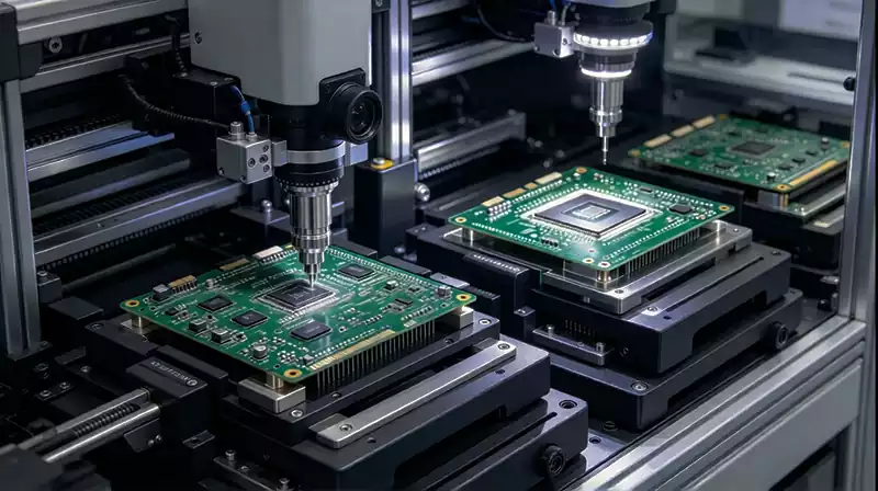
ICT and flying probe solve the same problem differently. ICT uses a bed-of-nails fixture with fixed probes and tests every board against it. It is the fastest per-board option in high volume, but the fixture is expensive and programming takes time, which makes it a poor fit for prototypes or product mixes. Flying probe moves a small set of probes, typically two, four, or eight heads, to each test point under program control. No fixture means no fixture cost, fast reprogramming, and coverage that often exceeds ICT on complex boards. The trade is speed: mechanical movement between points limits throughput, so flying probe does not belong on a high-volume line.
AOI is fast and blind. It scans the surface with high-resolution cameras and compares against the fabrication data, catching bridging, offset, missing parts, and polarity errors at high speed. What it cannot do is measure anything electrical. A perfect AOI pass says nothing about whether the nets connect.
AXI sees what nothing else sees. X-ray inspection is the standard method for verifying BGA solder quality and hidden joints, because optical methods cannot look under the package. It also validates microvia plating in HDI constructions. The cost is speed and money, which is why it is reserved for designs where hidden joints carry the reliability burden.
PCB testing at each stage of production
Where pcb testing happens matters as much as which methods you use. The governing principle is that defect cost multiplies downstream: a defect caught by AOI before electrical test costs a fraction of the same defect caught at final test, and industry experience puts that ratio in the order of ten times or more.
A typical bare pcb board sequence:
- After inner-layer etch — AOI on inner layers, before lamination buries them
- After drilling — hole presence and position checks
- After outer-layer etch — AOI on outer layers
- After solder mask — visual and dimensional verification
- After surface finish — solderability and coating checks
- Electrical test — flying probe or ICT, commonly on 100% of boards for high-reliability classes
- Final inspection — dimensional, visual, and packaging verification
Two sequencing rules are worth stealing from the assembly world even if you only buy bare boards. Test static before dynamic: verify continuity and isolation before applying power, because a powered short destroys the evidence. And test periphery first: the components at the edges of a board, where connectors, power, and protection devices live, fail more often than the ones in the middle.
How to choose the right PCB testing mix
Volume and reliability class drive the selection more than any other factor.
Prototypes and small batches. Flying probe plus manual visual. The math is simple: an ICT fixture for a 30-board run can cost more than the boards themselves, and flying probe gives you full electrical coverage with no fixture at all.
High-volume production. AOI plus ICT. AOI screens surface defects at line speed and ICT verifies every board electrically. This is the combination that keeps a 10,000-unit monthly run honest.
High-reliability programs: automotive, medical, HDI. The combination is not optional. Layer the methods: AOI for surface screening, flying probe or ICT for electrical verification, and AXI wherever BGA or hidden joints carry safety or performance weight. Programs in this class also test 100% of boards rather than sampling, because a sampling plan that passes on a safety-critical board is a sampling plan that failed.
What a real PCB testing report contains
If you are sourcing boards, the test report is where you find out whether testing happened or was assumed. A credible PCB testing report contains:
- The data basis: which Gerber and drill files the netlist was built from, so the test matches the revision you shipped
- The methods used: which methods ran on which boards, not a blanket claim of “fully tested”
- Coverage: what percentage of nets and test points the program actually reached
- Per-board results: pass/fail records tied to board serial or panel position, not a batch summary
- Defect data: what failed, where, and what was done about it, which is the raw material for process improvement
A report that says “all boards passed” without the data basis and coverage numbers is a report that cannot be audited. The difference shows up the first time a field failure needs a root cause.
Frequently asked questions about PCB testing
Is electrical PCB testing done on 100% of boards or on samples? It depends on the reliability class. High-reliability programs, including automotive and medical, test 100% of boards, and IPC-6012 Class 3 acceptance expects full electrical verification. Commercial and consumer programs may sample, trading coverage for cost. If your product’s failure cost is high, 100% is the only defensible number.
Can AOI replace electrical PCB testing? No. AOI is optical. It verifies what the surface looks like, not what the nets do. Opens, shorts, and incorrect net connectivity all pass AOI without difficulty, which is why AOI is always paired with an electrical method in serious programs.
Why is flying probe too slow for mass production? The probes physically move between test points, and that motion dominates the test time. On a prototype run of 30 boards it is irrelevant. On a line producing thousands of boards a day, ICT with a fixed fixture is orders of magnitude faster per board.
When is X-ray PCB testing actually necessary? When the joints you need to verify are hidden. BGA and other array packages conceal their solder joints from every optical method, and HDI microvias are too small to verify electrically in some constructions. If your design has neither, AXI is usually an expense you can skip.
PCB testing earns its cost by moving defects from the field back into the factory, where they are cheap. Specify the methods that match your volume and reliability class, insist on test data you can audit, and the boards that arrive will be the boards you designed.