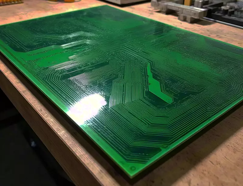
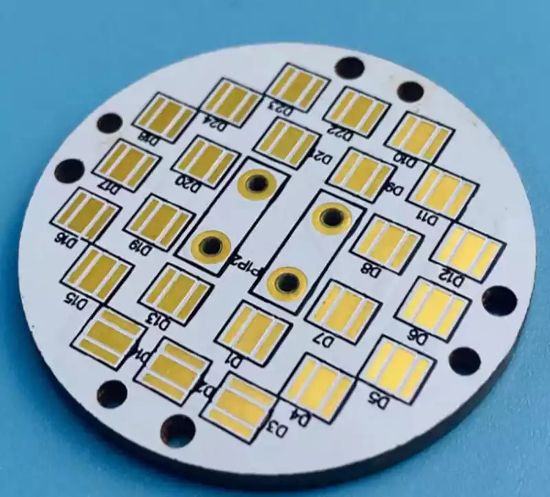
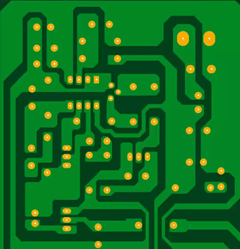
Bare PCB inspection is the process of judging an unassembled printed board against an acceptability standard, and IPC-A-600, Acceptability of Printed Boards, is the reference most often used for it. The standard fixes the target, acceptable and nonconforming conditions observable on the outside and inside of a bare board through photographs and illustrations, giving operators, inspectors and engineers a direct basis for accepting or rejecting product. The outcome decides whether a batch may enter assembly, and inconsistent interpretation makes incoming disputes hard to avoid.
How IPC-A-600 and IPC-6012 divide bare PCB inspection
Bare PCB inspection rests on two companion documents with separate jobs. IPC-A-600 is the acceptability standard. It describes target, acceptable and nonconforming conditions visible on the exterior or interior of a printed board, supplies illustrations, and sets out inspection items, minimum acceptance criteria and sampling frequency. IPC-6012 is the qualification and performance specification for rigid printed boards, stating performance requirements and numeric limits for the corresponding board constructions.
The performance specification comes first and the illustrated interpretation follows. IPC-A-600 supports and supplements the IPC-601X series as an inspection aid, and the standard does not recommend it as the performance specification for board manufacture or purchase. When an inspector judges the shape of an external defect, they turn to the illustrations in IPC-A-600. When they check a numeric threshold such as plated copper thickness or bow and twist, they return to the clauses of IPC-6012.
The three conditions and three classes of bare PCB inspection
IPC-A-600 defines three conditions for every characteristic. Target condition is the ideal state at the highest quality level. Acceptable condition permits minor deviation and allows release as long as product performance and reliability requirements are met. Nonconforming condition exceeds the acceptable range, affects performance, reliability or service life, and requires rejection.
The other prerequisite for bare PCB inspection is the product class, and the standard divides printed boards into three. Inspectors confirm the class before judging, because the same defect can be acceptable to very different degrees across classes.
| Class | Typical applications | Acceptance measure |
|---|---|---|
| Class 1, general electronic products | Consumer products, computer peripherals | Functional completeness is enough; appearance defects carry little weight |
| Class 2, dedicated service electronic products | Communications equipment, business machines, instruments | Performance and long life required; some appearance defects permitted |
| Class 3, high reliability electronic products | Military, medical, aerospace equipment | No downtime tolerated; strictest judgment |
How the bare PCB acceptance standard evolved from revision H to M
IPC-A-600 was first published in 1964 and ranks among the earliest IPC standards, with many revisions since. Revision H replaced G in April 2010. Revision J, issued in June 2016, added more than 120 illustrations covering microvias, plating voids and fill, and surface plating on edge connectors. Revision K replaced J in October 2020. The current revision M appeared in English in May 2025 and in Chinese in October 2025, a substantial structural upgrade. The sequence skips the letters I, L and O to avoid confusion.
Changes from K to M cluster in several areas. A dedicated acceptance rule for edge plating now covers coating uniformity, thickness, edge burrs and exposed copper. Qualification thresholds were added for bare pcb board cavities and back-drilled structures to suit high-speed and high-frequency back-drilling. Limits tightened for conductor thickness, local thinning, edge nicks and annular ring offset. Boundaries for plating voids, pinholes and missing plating in through holes and blind holes were refined by class. Rejection definitions were added for inner-layer separation, plating overhang and microcracks. The defect illustration set was fully updated to match IPC-6012F and IPC-6013E.
Systems still inspecting to revision H cite a document superseded three generations ago and out of step with current qualification standards. In a system audit or a customer factory review, that normally counts as a standards compliance deficiency.

Numeric limits for external defects in bare PCB inspection
Most external defect judgments come down to dimensional ratios. For annular ring, the minimum ring width on a supported hole is 50 micrometres for a Class 2 board and 75 micrometres for Class 3. An unsupported hole requires at least 150 micrometres, and an internally plated hole 25 micrometres. Breakout may not exceed 180 degrees on a Class 2 board or 90 degrees on Class 3.
White spots and microcracks below the base material surface are judged by whether they bridge conductors and by penetration depth. A microcrack may span no more than 50 percent of the distance between adjacent conductors, and its penetration at the board edge may not exceed 50 percent of the distance from the edge to the nearest conductor or 2.5 millimetres, whichever is smaller. Edge nicks use the same 50 percent or 2.5 millimetre limit. The longest dimension of a pit or surface void may not exceed 0.8 millimetres, affected area on one side may not exceed 5 percent, and the defect may not bridge conductors.
Plating voids in plated through holes are judged by class and show the clearest difference between Class 2 and Class 3.
| Defect | Class 2 judgment | Class 3 judgment |
|---|---|---|
| Copper plating voids | No more than one per hole; holes with voids no more than 5 percent; void length no more than 5 percent of hole length and less than 90 degrees of the circumference | No voids allowed in any hole |
| Minimum annular ring, supported hole | 50 micrometres | 75 micrometres |
| Breakout | No more than 180 degrees | No more than 90 degrees |
| Solder mask encroachment on land | No more than 50 micrometres where pitch exceeds 1.25 millimetres, and 25 micrometres where pitch runs from 0.65 to 1.25 millimetres | Same as Class 2; pitch below 0.65 millimetres by supplier and customer agreement |
For fine-pitch lands below 0.65 millimetres, the solder mask encroachment value is agreed between supplier and customer at every class, and the standard gives no single number.
Internal defects and microsectioning in bare PCB inspection
Some defects cannot be seen from the surface and need a microsection examined under a microscope. Sections are prepared after thermal stress testing. Inspectors examine copper foil and plating integrity in plated through holes at 100x magnification and perform arbitration examinations at 200x. Foil under 3/8 ounce may need 200x, with arbitration at 400 to 500x. Plating thickness below 1 micrometre is not measured by microscopical techniques.
Hole wall copper thickness has a specified minimum average and a single-point minimum by class. Classes 1 and 2 usually call for about 20 micrometres and Class 3 about 25 micrometres. Wicking limits tighten with class: no more than 125 micrometres for Class 1, 100 micrometres for Class 2 and 80 micrometres for Class 3. Delamination and blistering are normally rejected at every class. In the fill material of plated holes in metal core boards, wicking and radial cracks may not reduce the electrical clearance between adjacent conductive faces below 100 micrometres.
Flatness and dimensional limits in bare PCB inspection
Flatness is measured as bow and twist. To measure, inspectors place the board on a datum plane. Bow is calculated as the maximum rise along an edge minus board thickness, divided by edge length; twist is calculated as the height of the lifted corner minus board thickness, divided by diagonal length. Common limits are no more than 1.0 percent for Class 1, 0.75 percent for Class 2 and 0.5 percent for Class 3, with customer requirements taking precedence where they exist. Excess bow or twist causes placement offset, board jamming and poor solder joints, so the judgment basis belongs in the design stage alongside the assembly method.
Dimensional inspection covers board thickness, outline, hole diameter, conductor width and spacing, and hole position. Hole diameter is judged against drawing tolerance, and a conductor nick may not reduce width below the permitted ratio. Inspectors use graduated measuring tools so that results can be rechecked.
Inspection conditions and sampling for incoming bare PCB inspection
A judgment must be made under stated inspection conditions. External characteristics are normally viewed at 1.75x magnification with 3 dioptres of add, raised to 40x where detail cannot be resolved; the inside of a plated hole is examined at 100x and at 200x for arbitration. Inspectors normally hold the environment at 22 to 28 degrees Celsius, 40 to 70 percent relative humidity and 700 to 1200 lux, with the line of sight perpendicular to the sample and a straight-line viewing distance of 30 to 40 centimetres.
Sample size follows batch size. Incoming inspection commonly uses a single sampling plan, and defects are grouped as critical, major and minor, with zero acceptance for critical defects. Appearance, dimensions, adhesion and microsections each carry their own sample size and acceptance level, and microsectioning normally takes one coupon per batch. Supplier shipments should include solderability, cleanliness, dimensional and microsection reports; a missing report or a failed item in any of them allows the incoming inspection to reject the batch.
Common questions about bare PCB inspection
Can IPC-A-600 and IPC-6012 replace each other in bare PCB inspection. They cannot. The first gives illustrated judgments for externally and internally observable characteristics and supports inspection work; the second states performance requirements and numeric limits. Use the first for defect shape and the second for numeric thresholds.
How should inspection records that still cite revision H be handled after revision M takes effect. Recheck every document that references IPC-A-600, update entries marked H, J or K to revision M, bring in companion standards such as IPC-6012F and IPC-6013E, and revise internal inspection specifications and incoming criteria.
Does a bare pcb board that passes visual inspection still need microsectioning and electrical testing. It does. Internal defects such as delamination, plating voids and wicking cannot be identified from appearance and require a microsection; conductor continuity is likewise beyond visual inspection and needs electrical testing. Visual judgment covers observable characteristics only.
Disputes over bare PCB inspection usually trace back to a class and revision that were never fixed at the purchase stage. Put both in writing and receiving inspection has a shared basis.