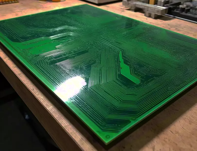
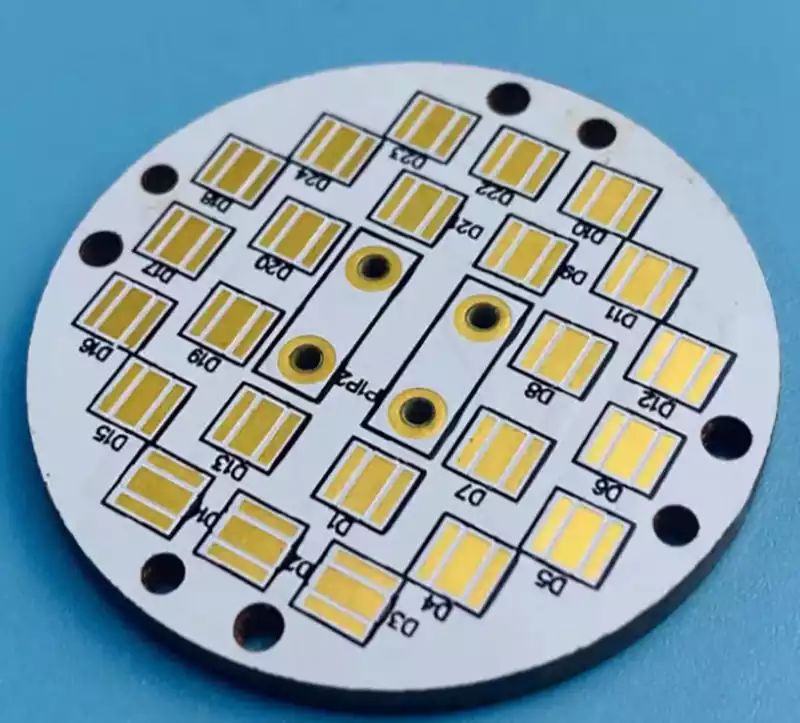
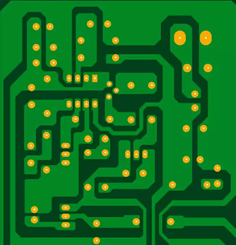
A bare PCB is a printed circuit board that has completed circuit patterning and surface finish but carries no mounted components. It is also called a bare board, an unpopulated board or an unassembled board, and it belongs to a different stage of the production chain from a finished assembly. A bare PCB consists of the substrate, copper foil traces, solder mask, silkscreen, pads and vias.
It performs no circuit function on its own; its purpose is to carry later assembly and provide electrical connections and mechanical support. The quality of a bare PCB is already fixed before assembly, and conductor continuity, hole wall plating, solder mask coverage, surface finish and dimensional tolerance all have to be verified at receipt. If these issues are left until after component mounting, rework cost and delivery time rise sharply.
The layer structure of a bare PCB
A bare PCB is built by pressing together several types of material. The substrate supplies stiffness and thickness. The common type is glass-fibre-reinforced epoxy; flexible boards use polyimide film, and metal-core and ceramic substrates serve applications with high heat-dissipation requirements. Copper foil is bonded to the substrate surface by heat and pressure. A double-sided bare PCB has one copper layer on each face, while a multilayer board alternates more copper layers with prepreg. Copper thickness is measured in ounces per square foot. One-third ounce is about 12 micrometres, half an ounce about 18, one ounce about 35 and two ounces about 70. High-power boards use heavier copper.
Above the copper layers sits the solder mask, which covers the traces to prevent solder bridging and protects the copper from moisture and electrolytes. The mask leaves windows at pads and hole annuli for soldering. Green is the most common colour, though black, white and red are also used. The outermost layer is silkscreen, which marks component positions and reference designators for assembly and repair. A bare PCB also carries several functional features: pads for soldering components, plated through holes that connect traces on different layers, and gold fingers, the exposed gold-plated contacts along a board edge used for plug-in connections.
Bare PCB materials and classification
A bare PCB can be classified by substrate, rigidity and number of conductive layers. By substrate there are organic and inorganic materials. Organic materials include phenolic resin, glass-fibre epoxy, polyimide and BT resin, and account for the great majority of circuit boards. Inorganic materials are mainly aluminium, copper and ceramic substrates, whose defining feature is heat dissipation.
By rigidity, boards are rigid, flexible or rigid-flex. Flexible boards can bend and are used where space is limited or repeated flexing is required. By conductive layer count, boards are single-sided, double-sided or multilayer. A multilayer bare PCB is pressed from several core sheets and prepreg, and higher layer counts demand tighter registration and interlayer reliability.
Layer count and via technology give rise to through-hole boards and first- and second-order high-density interconnect boards. A via in a through-hole board runs from the first layer to the last regardless of layer count, so a twenty-layer board can still use through vias throughout. Higher-order products form laser-drilled blind vias in the surface and build up layer by layer, raising process complexity and cost. The choice follows circuit complexity and routing density.
Bare PCB surface finish types
Exposed copper oxidises in air, and the oxide layer prevents solder from bonding, causing poor wetting and cold joints. A bare PCB therefore receives a surface finish before it leaves production, balancing solderability against storage stability. Seven common finishes differ markedly in solderability, flatness and shelf life. Hot air solder leveling dips the board in molten solder and blows the surface flat with hot air; it comes in leaded and lead-free forms and is low in cost with good solderability.
The organic solderability preservative forms a thin organic film over the copper, offering good flatness and coplanarity for fine-pitch placement but limited heat resistance. Electroless nickel immersion gold deposits an electroless nickel-phosphorus layer followed by immersion gold, giving a flat surface, long shelf life and tolerance of multiple reflow cycles. Electroplated nickel gold, immersion silver, immersion tin and hard gold plating on gold fingers serve plug-in contacts, repeated soldering operations or special electrical requirements.
Finish selection follows the application. Cost-sensitive assemblies with wide pin spacing use hot air solder leveling or the organic solderability preservative; fine-pitch devices that demand flatness use electroless nickel immersion gold, immersion silver or immersion tin; contacts subject to repeated mating use electroplated gold. The surface finish also determines the shelf life of a bare PCB.
Engineering data preparation before bare PCB production
Before a bare PCB enters production, the Gerber files, drilling data and netlist supplied by the customer must be processed by the factory engineering department into instructions that each process can execute. The first step is to load the data into a CAM system and check that all layers are present and aligned, examining the mechanical outline, drill map, routed slots, inner and outer circuit layers, solder mask and legend artwork item by item.
The review focuses on whether line width and spacing, hole diameter, pad annulus, stack-up and impedance requirements fall within the factory process capability. Common problems involve wrong file revisions, unreasonable impedance designs and mismatched pad dimensions. Items in question are returned to the customer through an engineering query list and confirmed before the next step.
Stack-up confirmation converts the customer design layer order into a structure that can be pressed. The factory recalculates the dielectric thickness and corresponding trace widths for each layer using its own materials and lamination capability, and returns the stack-up and impedance calculations to the customer for approval. Where the difference is small, production follows the factory figures. A multilayer stack-up is symmetric about the centre layer, with copper and dielectric thickness mirrored on opposite sides; otherwise heating during lamination and reflow is uneven and warpage is likely.
The CAM engineer edits the drill program from the Gerber data, setting drill attributes and tool compensation. For a component hole, for example, the drill size is increased so the finished hole meets its specified diameter and tolerance. During editing, the spacing on the panel, the number of tool changes, the hit count for each tool and the total number of holes and slots are checked against the manufacturing instructions.
The drill file must use the same units and precision as the Gerber data, or holes will be offset from the centre of their pads. The artwork is also compensated for etching and solder mask: design line widths are widened in advance by the etch factor to offset the narrowing that occurs during etching.
Test programs and fixtures are prepared at the same stage. Production panels use a bed-of-nails fixture built to the test-point grid, while prototypes and small batches use a flying-probe program. The netlist serves as a cross-check: the CAM system generates a reference netlist from the plotted artwork and compares it with the customer netlist to detect opens, shorts and artwork anomalies.
Panelisation determines material utilisation and downstream handling efficiency. The factory arranges the customer small boards into a standard production panel, leaving sufficient spacing between boards and adding process rails and tooling holes for machine clamping and registration. The panel layout directly affects the material cost allocated to each board; excessive spacing or irregular nesting increases offcut losses.
For boards requiring controlled impedance, the factory places test coupons along the edge of the production panel. A coupon replicates the layer stack, trace width and spacing and reference planes of the board itself for TDR measurement. Probe spacing on the coupon is fixed to the requirements of the test equipment. Coupons are normally removed before shipment, and what accompanies the board is an impedance test report.
Once the data are complete, the engineering department carries out an internal check and then passes the Gerber files, manufacturing instructions and drill program to a quality engineer for review. Production starts only after approval. If drilling offsets, etching defects or insufficient solder mask exposure appear during production, engineering returns to the data to determine whether the cause lies in the data or in process setup.
Industry standards for bare PCB acceptance
Acceptance of a bare PCB at receipt is judged against published industry standards; visual impression serves only as a preliminary reference. Two documents are used together. IPC-A-600 is the acceptability standard for bare board appearance, providing visual criteria for more than a hundred inspection items covering hole copper, copper foil defects, solder mask, legend and substrate, with target, acceptable and nonconforming conditions.
IPC-6012 is the performance and qualification specification for rigid boards, setting quantitative thresholds for hole copper thickness, warp and dimensional tolerance by product class. The first supplies the illustrated criteria and the second the measured values, and the two are normally cited together. Products are divided into three classes: Class 1 for general electronics, Class 2 for dedicated service equipment and Class 3 for high-reliability equipment. A higher class allows fewer defects.
Solder mask appearance illustrates the difference between Class 2 and Class 3. Under Class 2 the solder mask over a lead is at least 8 micrometres thick, while Class 3 requires 10 to 15 micrometres. Mask registration tolerance is plus or minus 3 mil for Class 2 and tightens to plus or minus 2 mil for Class 3. Class 2 permits slight offset of the solder mask dam as long as it does not break; Class 3 permits no defect, and plugged vias must be flat at the opening with no recess.
Incoming inspection normally grades defects as critical, major or minor and uses a sampling plan: the acceptance number for critical defects is zero, the common acceptable quality level for major defects is 0.4 and for minor defects 1.0. For internal defects such as delamination and blistering, the acceptable condition limits the affected area to no more than 1 percent of one side of the board, the span to no more than 25 percent of the spacing between adjacent conductive features, and the distance from the board edge to at least 2.5 millimetres.
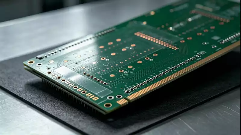
Electrical continuity testing of a bare PCB
Visual acceptance does not prove that the circuitry is continuous. A bare PCB also undergoes electrical testing to confirm that every net conducts and that nets are insulated from one another. This step is completed before assembly to eliminate inherent opens and shorts. Two main methods are used, chosen according to volume and fixture cost. Bed-of-nails testing uses spring-loaded probes on a fixed grid to contact all test points at once, with probe force generally between 100 and 200 grams and common grid pitches of 100, 75 or 50 mil.
It measures thousands of points in one pass, often taking only tens of seconds per side, but requires a fixture for each board type, making it costly and suited to high volume. Flying-probe testing uses two to eight movable probes driven directly by computer data to step from point to point, with a minimum test gap down to 0.2 millimetres and probe positioning accuracy of 5 to 15 micrometres. It needs no fixture and changes over quickly, which suits prototypes and small batches; the trade-off is speed, since one board may take eight to ten minutes or even an hour, and board size is usually limited to 16 by 24 inches.
The test grid also constrains design. A 2.5-millimetre grid requires test pads at least 1.3 millimetres in diameter, and a 1-millimetre grid requires at least 0.7 millimetres; too fine a grid makes probes fragile. Besides continuity testing, a bare PCB may undergo insulation and withstand-voltage testing to verify dielectric strength between conductors. Inspection is typically organised in three layers, with bare board inspection first and in-circuit and functional testing after assembly; the earlier a defect is found, the less it costs to correct.
Bare PCB shelf life and moisture handling
After a bare PCB leaves the line, both the surface finish and the substrate degrade with time, so storage conditions determine whether the board is still usable when it reaches assembly. Storage requires 10 to 30 degrees Celsius and relative humidity no higher than 75 percent, away from direct sunlight and acidic or alkaline corrosive gases. Bare boards are generally shipped vacuum-packed with desiccant and a humidity indicator card inside.
The card shows whether the package has failed; before use, its reading must be within limits, and a damaged packet or a changed card calls for treatment. With the vacuum package intact, shelf life varies widely by finish: an OSP board is typically about three months, an electroless nickel immersion gold board about six months, and a hot-air-solder-levelled board up to one year, with the supplier specification taking precedence.
Moisture is the hazard. When a bare PCB is heated above 100 degrees Celsius in reflow or wave soldering, internal moisture turns to steam and expands. If it cannot escape quickly enough, it can force the layers apart, causing delamination, blistering or even board burst, and in severe cases break a plated through hole. Internal damage not visible on the surface can lead later to electrical instability and ion migration.
Boards stored beyond their shelf life or with a failed package therefore need baking before assembly. A common practice places the baking temperature around 120 degrees Celsius for one to six hours depending on storage time, while some argue for gentler drying around 105 degrees Celsius to reduce oxidation risk. The baking temperature must stay below the glass transition temperature of the laminate. OSP boards are generally not baked, because heat degrades the protective film; a moisture-damaged OSP board is usually returned to the supplier. Baked boards should be consumed within a specified time, or repackaged or baked again.
Common bare PCB defects and their causes
Defects in a bare PCB fall into five groups: conductor pattern, plated holes, solder mask coverage, interlayer bonding and outline dimensions. IPC-A-600 provides target, acceptable and nonconforming illustrations for appearance defects, while IPC-6012 specifies quantitative thresholds such as hole copper thickness, warp and dimensional tolerance by product class. Together the two documents define the boundary of acceptability.
Defects of the conductor pattern and plated holes appear as opens, shorts and incomplete hole wall plating. A local break in a trace or a bridge between adjacent nets usually originates in artwork transfer and etching deviations; burrs from drilling, insufficient desmearing or uneven electroless copper leave voids in the hole wall and poor interlayer continuity. These defects cannot be seen by eye and require bed-of-nails or flying-probe continuity testing to confirm that each net conducts and nets remain insulated.
Solder mask and legend defects belong to visual acceptability and include broken solder dams, mask misregistration, recessed plugged vias and insufficient ink thickness. The mask leaves windows at pads and hole annuli; when coating or alignment drifts, a shifted window exposes a soldering area or destroys isolation between adjacent pads. Class 2 and Class 3 products set different acceptable conditions for these items, and incoming inspection grades defects as critical, major or minor under a sampling plan.
Delamination, blistering and board burst occur in the substrate and between layers. Heated above 100 degrees Celsius in reflow or wave soldering, a damp board develops expanding vapour that forces the layers apart and may break plated holes. Such damage is hard to detect initially and leads later to electrical instability and ion migration. Vacuum packing, humidity indicator cards and baking before assembly keep moisture risk within acceptable limits, but once the defect has formed, baking cannot remove it.
Outline defects are mainly warp and dimensional tolerance overrun, associated with uneven lamination stress and deformation during thermal processing and judged against the quantitative thresholds of IPC-6012 for the relevant class. Grouping bare PCB defects by cause allows the incoming inspection method to be matched to each group: conductor and hole defects by electrical testing, solder mask and legend defects by visual judgement, and interlayer and dimensional defects by visual inspection combined with measurement.
Common questions about bare PCB delivery
What is the difference between a bare PCB and an assembled board. A bare PCB carries no components and performs no circuit function; it is the carrier for connection and support. An assembled board has all devices soldered onto the bare board and executes the designed function when powered. The two belong to different production stages, supply chain steps and acceptance criteria.
Does a visually perfect bare PCB still need electrical testing. Yes. Micro-breaks inside a conductor, plating defects in the hole wall and insulation problems between adjacent nets cannot be seen by eye and are found only by electrical testing, so continuity testing must be completed before assembly.
Can a bare PCB past its shelf life still be used. It depends on the surface finish and storage condition. A board with an intact package and a humidity card within limits can continue in use after confirmation; one stored too long or exposed to moisture needs baking, and a moisture-damaged OSP board is returned to the supplier for treatment. Even after baking, the surface finish and interlayer bond have degraded, which carries a long-term risk.
The quality of a bare PCB is fixed at receipt, and assembly only carries that conclusion out. Inspection is done early because rework later costs far more.