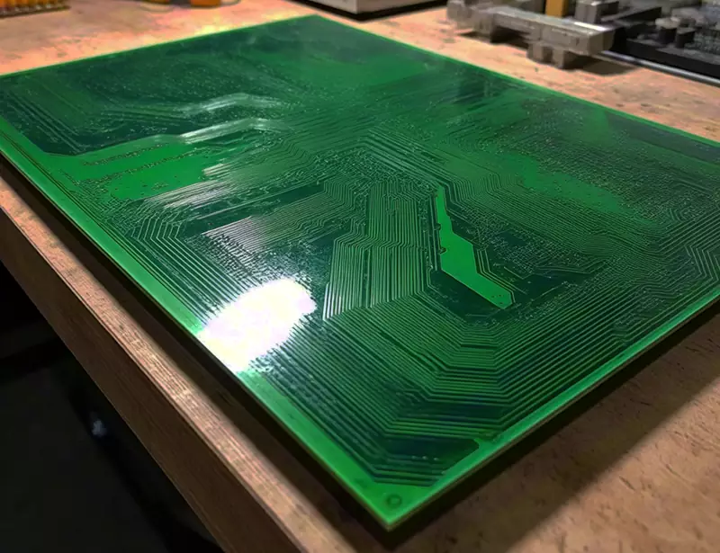
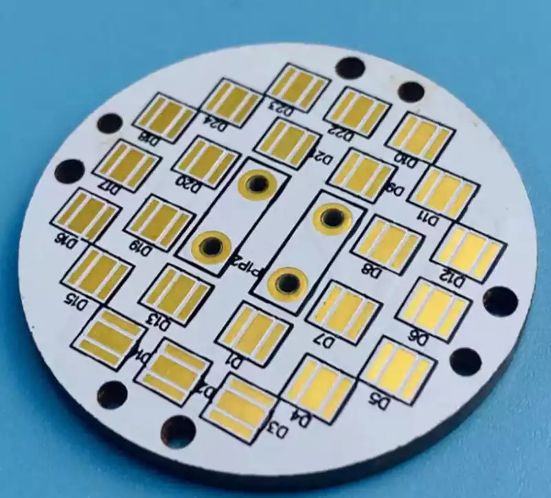
The number on a multilayer PCB quote is a sum. It starts with a one-time engineering fee, adds material, process, testing, special-process and lead-time charges, then subtracts any volume discount. Fabricators price by order area, and that area comes from the delivered panel size divided by the number of strips per panel and multiplied by the order quantity. Two boards with the same outline can carry very different unit prices once the panel layout and the order size change. What a designer can do is identify the items on that sheet that are open to adjustment, and decide before prototyping which ones are worth paying for.
The same file often draws different quotes from different fabricators. The gap usually sits in how each one counts, since every shop starts from a standard sheet, fits a different number of panels into it, and carries its own scrap and process capability. Reading a multilayer PCB quote item by item shows exactly where the numbers part company.
Engineering fees and the material base of a multilayer PCB
The engineering fee covers film generation, program writing and a manufacturability review. It is a one-time charge, collected again on each revision, and repeat orders of an unchanged version can often be waived. Material cost in a multilayer PCB starts with the copper-clad laminate and prepreg. Standard FR-4 is the baseline. A high-Tg laminate runs 8 to 10 percent above a standard-Tg one, and a mid-Tg grade about 3 to 5 percent above.
High-frequency laminates cost several times as much as ordinary ones. A 1.6 mm board is the common thickness, and every 0.4 mm away from it moves the cost by 30 to 40 yuan per square meter. One-ounce copper is standard, and moving to two ounces adds 60 to 90 yuan per square meter.
Layer count multiplies both material and process. Taking a two-layer board as 1, a four-layer board runs about 1.8 to 2.5 times and a six-layer board about 3 to 4 times; above eight layers the rise approaches exponential. Each added layer repeats lamination, registration, inner-layer imaging and drilling, and it lifts the scrap risk along with them.
- Cost-adding move: adding two spare layers for margin, using two-ounce copper across the whole board, and defaulting to high Tg where no thermal demand exists.
- Cost-saving move: tightening the routing until the layer count is just enough, setting copper weight by current region, choosing Tg by the actual number of reflow passes, and holding thickness in the common 1.2 to 1.6 mm range.
Drilling and hole structure costs in a multilayer PCB
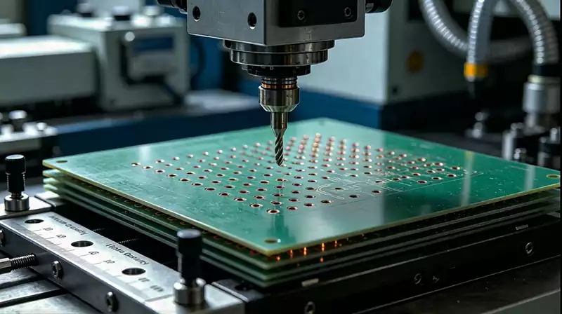
Drilling is priced by hole count and diameter. A typical through-hole density is around 100,000 per square meter, and some lines count 200,000. At a 0.3 mm diameter, every extra 10,000 through-holes per square meter adds 3 to 5 yuan. Smaller drills break more easily and tighten the aspect-ratio limit. A 0.2 mm drill normally suits boards no thicker than 1.6 mm, while a 0.3 mm drill holds an aspect ratio near 12 to 1; beyond that, pulse plating equipment is required.
Blind and buried vias are priced separately. In a multilayer PCB, each additional blind or buried via type adds at least 200 yuan in engineering fees, and the holes themselves cost 30 to 60 percent more than through-holes. The manufacturable spacing limits matter at the same time: keep via edge to via edge at 6 mils or more, preferably above 8 mils; keep pin-hole to pin-hole at 0.3 mm or more; keep pad to board outline at 0.2 mm for vias and 0.25 mm for pin-holes; keep non-plated slots 1.6 mm apart and 2 mm from the board edge. Tight spacing brings broken holes, wicking and ion migration, and rework costs far more than the area it saves.
- Cost-adding move: using blind and buried vias where through-routing would work, driving diameters ever smaller, and pressing spacing down to the process floor.
- Cost-saving move: using through-holes wherever they route cleanly, setting diameters by current and assembly margin, and leaving spacing wider than the minimum.
Fine-line and impedance charges in a multilayer PCB
Trace and space at 0.1 mm and above is ordinary process in a multilayer PCB. Dropping to 0.05 mm calls for laser direct imaging and a clear step up in cost. The industry treats lines under 0.15 mm, microvias under 0.2 mm and laser drilling as fine-feature work, with a 20 to 40 percent processing surcharge and a higher scrap rate. Impedance control is charged per group, about 50 yuan per batch per group for testing, and the test coupons also take up panel area. Solder-mask dams should be at least 4 mils wide, and 6 mils for high-reliability work.
- Cost-adding move: designing the whole board at the finest line width and attaching an impedance requirement to every net.
- Cost-saving move: confining fine lines to dense fan-out areas, holding ordinary widths elsewhere, and applying impedance only to the signal groups that need control.
Panel utilization and the billed area of a multilayer PCB
Fabricators start from a large sheet, commonly 1220 by 1030 mm, and bill the full sheet opened for the order. The net area of one board does not set the price on its own. A smaller or oddly shaped board leaves fewer units in the sheet and more scrap at the edges, so the unit price climbs. A conventional two-layer board is normally expected to use 80 percent or more of the sheet, and a multilayer PCB 75 percent or more. Below that, cost rises. Better panel layout and test coupons placed to fill space can cut 5 to 15 percent from the cost.
Panelization carries its own rules. Units under 50 by 50 mm suit panelizing, and a combined panel should stay within 330 by 250 mm. Of the separation methods, V-groove is cheapest at usually under 1 yuan per square meter, while routing runs 0.5 to 2 yuan. V-grooves need board thickness of 2 mm or less with a 1 mm keep-out on each side. Stamp holes commonly use a 1 mm diameter at 1.27 mm pitch, and ball-grid-array pads should sit at least 20 mm from a V-groove or stamp-hole line so that depaneling stress does not crack joints.
- Cost-adding move: outlines with irregular cutouts, single boards ordered as singles, and routing for every separation.
- Cost-saving move: keeping outlines regular, panelizing small boards, taking V-grooves where they fit, and counting panel numbers into the quote up front.
Surface finish, testing and lead-time extras in a multilayer PCB
Surface finishes run from low to high cost through anti-oxidation, hot-air solder leveling and immersion gold. Immersion gold costs 25 to 50 percent more than solder leveling, and earns its place when fine-pitch parts need a flat pad. Green solder mask is the cheapest. White and black add ten-plus yuan per square meter, and special colors add more. Testing is charged by method. Flying-probe testing runs about 0.01 to 0.03 yuan per point and suits prototypes. Above a certain quantity a fixture is opened, costing 300 to 1000 yuan once and working out cheaper per board. Raising the inspection level by one grade doubles the sampled share and adds 10 to 20 percent to cost.
Lead time and quantity close the list. Standard lead time is 10 to 30 days. Each 1 to 2 days shaved off adds a 10 percent rush fee, and a 24- or 48-hour run can carry 20 to 100 percent on top. Multiplying the quantity tenfold can drop the unit price 30 to 40 percent, since engineering and fixture fees spread over more boards.
- Cost-adding move: immersing gold on a coarse-pitch board, opening a fixture for a small batch, defaulting to the top inspection grade, and ordering close to the needed date.
- Cost-saving move: matching finish to the assembly process, letting test method follow batch size, setting inspection grade by the cost of failure, and building to the standard queue.
A line-by-line cost comparison of a multilayer PCB
Put the choices above into one sheet and every item has an expensive end and a cheap end.
| Cost item | Cost-adding move | Cost-saving move |
|---|---|---|
| Layer count | two spare layers for margin | routing tightened to what is needed |
| Material | high Tg and high-frequency by default | grade set by measured need |
| Copper weight | two ounces across the board | copper set by current region |
| Hole structure | blind and buried vias, micro-holes | through-holes at sensible diameters |
| Trace and space | finest lines across the board | fine lines local, ordinary elsewhere |
| Impedance | added to every net | added to critical groups only |
| Panelization | odd outline ordered as singles | regular outline, more units per sheet |
| Separation | routing for every board | V-grooves wherever they fit |
| Surface finish | immersion gold on coarse pitch | finish matched to assembly |
| Lead time | 24-hour rush | standard queue |
No line is right or wrong on its own. The point of checking each one is to remove capabilities the design never uses from the quote, while keeping the parts that carry real reliability.
Common questions about multilayer PCB cost and design choices
Why does a four-layer board cost more than twice a two-layer board?
Price follows process steps, not board area. A four-layer board adds lamination, registration and inner-layer imaging to the two-layer flow, and each step brings material, labor and scrap risk, so the link between layer count and price looks closer to multiplication.
Why does a small oddly shaped board cost more than a larger regular one of the same area?
Fabricators lay out a full sheet. An odd outline or a small unit fits fewer pieces into it and leaves more scrap at the edges. For the same net area, the sheet holding the low-utilization design is spread over fewer finished boards, so the unit price goes up.
Why is immersion gold not always the better choice?
Immersion gold buys a flat pad at a price well above solder leveling. On a board with wide lead pitch and no need for a flat assembly surface, immersion gold pays for a capability the design does not use. Settle the assembly requirement first, then decide the finish.
A multilayer PCB quote deserves a request for an itemized sheet, with engineering, material, process, testing, extras and lead time each matched against the design file. Where an item maps to a capability the design never uses, take it out of the next revision. Reading that sheet closely does more for the final cost of the board than pushing on the unit price alone.