Warpage is the deviation of a multilayer PCB from a flat reference plane. It shows up as either bow, a uniform cylindrical curvature, or twist, a saddle-shaped distortion. The industry measures and accepts it against IPC-6012 and IPC-TM-650. Surface-mount (SMT) boards are generally allowed up to 0.75% maximum warpage, while other printed boards usually stay within 1.5%. In practice, assembly houses often tighten the limit to 0.70%–0.75%. Boards with flatness-sensitive packages such as BGA and SMB commonly require less than 0.5%, and some orders even specify under 0.3%.
Warpage is expressed as warp height divided by the chord length times 100%, and often reported as the height of a single corner divided by twice the diagonal length. When warpage runs high, pick-and-place machines cannot release components at a constant height. The board’s changing flatness during reflow lets parts drift on the molten solder, causing bridges or open circuits. PCB boards that exceed the assembly house limit can also develop solder-joint cracks after reflow, pulling down the yield of the whole batch.
Warpage is among the most common and hardest-to-eliminate defects in multilayer PCBs during lamination and reflow. Symmetric stackup design is the main way to suppress it. By treating the finished board’s centerline as the mirror axis, the materials, dielectric thicknesses, and copper distribution on the top and bottom halves are made as close to mirror images as possible, so the stresses built up during pressing and cooling cancel out. This article follows that line to explain how warpage forms, how to check a stackup for symmetry, and the engineering trade-offs when perfect symmetry is out of reach.
How asymmetric stackup creates warpage forces in multilayer PCBs
In a multilayer PCB, heating, resin flow, cure shrinkage, and cooling during lamination happen almost at once. Copper, glass fiber, and epoxy differ sharply in thermal expansion and cure shrinkage. Copper has a coefficient of thermal expansion (CTE) around 17.7 ppm/°C, glass cloth about 2.9–5 ppm/°C, and epoxy resin as high as 67.1 ppm/°C. For FR-4 laminate, the Z-axis CTE sits at 50–70 ppm/°C below Tg and jumps to 250–350 ppm/°C above it.
During heated lamination the materials are constrained in the plane, but once cooled, different shrinkage on the two sides of the centerline produces a bending tendency like a bimetallic strip. The closer the mismatch sits to the outer surface, the longer the moment arm and the stronger the bending force. So matching the total layer count, overall thickness, and outer copper weight does not prove a balanced stackup. Equal total copper does not mean equal stress distribution across the centerline.
Four fields to verify when checking multilayer PCB symmetry
To judge symmetry in a multilayer PCB, use the finished board’s centerline as the boundary and compare each layer in the top half against its counterpart in the bottom half. Matching signal layer to signal layer and plane layer to plane layer is only the start. You also check these four fields:
- Material pairing: the core, prepreg (PP), and resin system on corresponding layers should match.
- Thickness pairing: measure the dielectric distance to the centerline on corresponding layers, including core thickness and the number of PP sheets.
- Copper distribution: look at both the average copper coverage of a whole layer and the local copper density. Paired layers and zones should both balance.
- Pattern distribution: the type of distribution on large copper-foil layers and on trace layers should correspond on both sides.
These fields do not all need to match exactly, but any asymmetry in a multilayer PCB must have an electrical or manufacturing reason. When a power plane and a ground plane carry different copper areas, you can reduce the difference with copper-balancing patterns, scrap-edge copper fill, or resequencing the layers. Any added copper must respect clearance and net rules. You should not place floating copper near high-speed nodes or change the impedance boundary.
Common pseudo-symmetric structures in multilayer PCBs
A drawing may show symmetric layer numbers while the material stack is not symmetric. The following types of pseudo-symmetry commonly appear in multilayer PCB design.
Dielectric thickness asymmetry: when the L1-2 dielectric is far thicker than other layers and multiple 7628 sheets are used to control cost while adjacent layers use only a single 2116, the different expansion coefficients of the two PP types bow the board sharply toward the solder side. Switching to multiple 2116 sheets that match the core and other layers brings the glass styles closer and reduces warpage.
Blind-via structural asymmetry: in a stackup like (1+2)+2+1, layers 1–3 are first pressed and drilled as blind vias, so the second press effectively becomes an asymmetric 2+2+1 structure that warps with high probability. Without changing the dielectric requirements, switching to a truly symmetric (1+2)+(2+1) stackup markedly lowers the risk.
Mixed-material asymmetry: when a high-frequency laminate is pressed together with FR-4, different material CTEs still produce directional warpage even if the core thickness and base copper look similar. Prioritize material symmetry in the stackup. If that is impossible, tune the lamination cool-down rate instead.
Scrap-edge asymmetry: when the scrap edge fully surrounds the inner pattern, the copper-residual difference between the two builds residual stress and warps the scrap edge. Counter it with copper fill or balancing dots in the scrap area, and add hang points or breakaway holes evenly to raise rigidity.
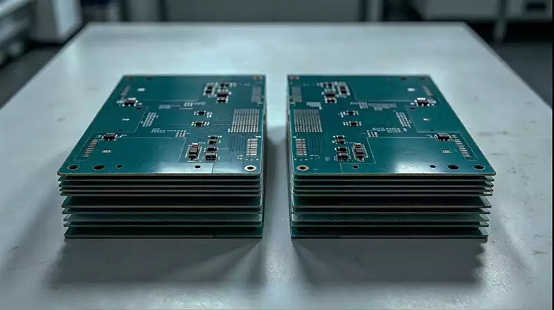
Verifying the effect of symmetric stackup on multilayer PCBs
A symmetric stackup lowers the warpage risk of a multilayer PCB, but it does not guarantee a perfectly flat board in every design. Ultra-thin boards, extra-large panels, local heavy copper, mixed materials, embedded copper blocks, and uneven component thermal mass all introduce new structural differences that the fabricator still needs to evaluate against its actual process.
To quantify the effect of a symmetric multilayer PCB stackup, keep the same laminate batch, outline, total thickness, and press parameters, and change only the stackup toward a closer mirror image while holding the artwork and surface finish fixed. Record bow and twist after pressing, after completion, and after reflow, with fixed measurement points on the panel scrap edge and the finished diagonal. A single visual check for flatness cannot replace quantification. The change after temperature cycling shows more clearly whether residual stress is still releasing.
Compromises when a multilayer PCB cannot be fully symmetric
Real requirements from customers for dielectric thickness, impedance, and signal integrity in a multilayer PCB often make a perfect mirror impossible. The reliable approach is to satisfy the electrical function first, then balance the materials and copper distribution around the centerline as much as possible, and record the reason for any asymmetry in the stackup note and the inspection plan.
Specific anti-warpage measures are adopted as follows: copper-clad laminates are pre-baked at 150°C for 8 ± 2 hours prior to cutting to eliminate internal stress and moisture. In lamination, the warp and weft directions of PP sheets are aligned uniformly, with the machine direction defined as warp and the cross-width direction as weft. After hot and cold pressing, panels undergo a 4-hour flat resting stage inside a 150°C oven for stress relief. During plating, 0.4–0.6 mm thin substrates are straightened via roller traction.
After hot-air leveling, boards are cooled naturally on flat steel plates. For 16-layer and heavier stacks, gradient cooling is implemented: the temperature drops sequentially from 220°C to 180°C and then to 150°C, with a 20–30 second dwell at each stage. High-Tg base materials with Tg ≥ 170°C are also specified to mitigate softening during reflow.
A stepwise pressing scheme paired with a controlled ramp rate of 3–5°C per minute is applied. Compared with conventional manufacturing cycles, this approach reduces interlayer residual stress by approximately 38%.
Common questions about warpage and symmetric stackup in multilayer PCBs
At what copper-residual difference does warpage start to rise noticeably? When the copper area differs by more than 40% between the two sides of a multilayer PCB, the warpage rate rises sharply. In design, keep the copper residual of inner and outer layers as close as possible. When the gap is large, balance it with independent meshes or scrap-edge copper fill.
How should odd-layer or asymmetric HDI structures be handled? The blind-via flow in multilayer PCB HDI easily forms pseudo-symmetry. Adding one more inner-layer press to make a truly symmetric stackup helps, and mixed-material structures should prioritize material symmetry. If symmetry is truly impossible, state the reason in the stackup note and rely on process controls such as gradient cooling.
Can baking or correction fully remove warpage? Baking releases only part of the residual stress and cannot fully remove warpage. PCB boards out of tolerance can be flattened with a bow-shaped mold hot press or a pneumatic straightener, but some springback remains after correction. The real control still lives at the design stage.
The starting point for controlling warpage in a multilayer PCB is the stackup table. Fold it once along the board’s centerline and find, item by item, the materials and copper distributions that lack a mirror relationship. That beats staring only at total thickness. Make symmetric stackup a fixed step in design review, and record the reason for any unavoidable asymmetry in the stackup note, so you get a reliable result between electrical performance and manufacturing flatness.