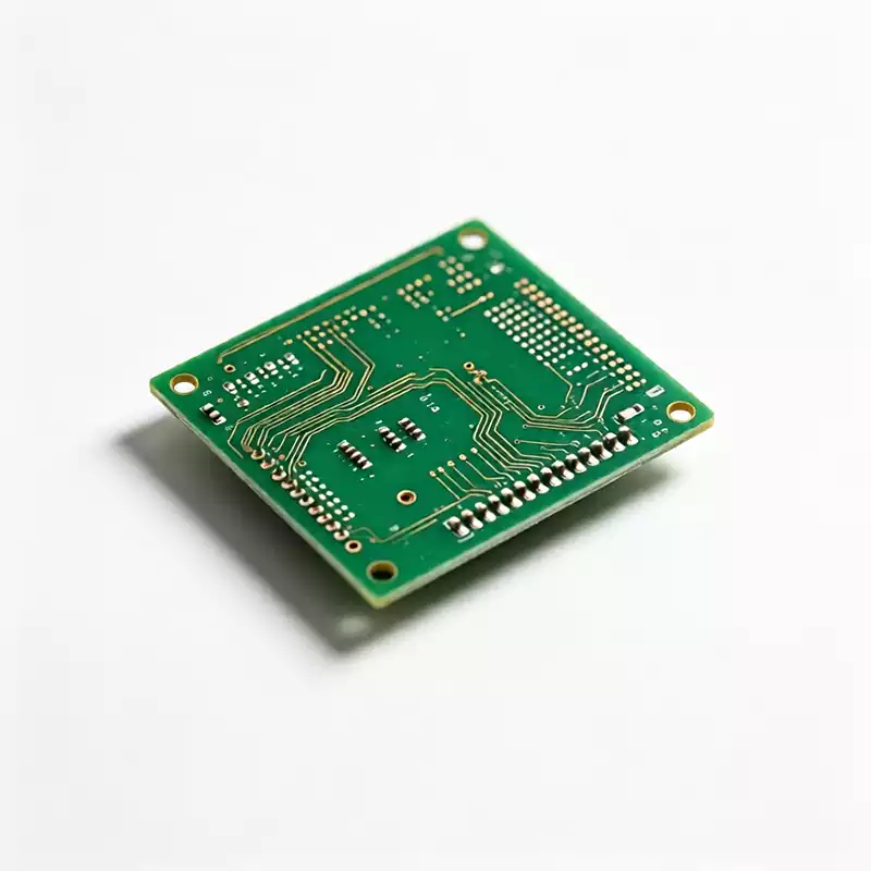
Choosing an hdi pcb stackup is the decision that quietly sets your cost, lead time, and yield before a single trace is drawn. The notation 1+N+1, 2+N+2 and any-layer looks like a menu, but each step up the ladder adds lamination cycles, copper-fill requirements, and process risk that you cannot undo after layout is locked. This guide turns the menu into a selection path you can run from your own BGA pitch and routing demand, not from a vendor brochure.
What the numbers actually mean
The notation describes how many high-density build-up layers sit on each side of a conventional core. In 1+N+1, the two outer “1”s are single build-up layers laminated onto each side of an “N”-layer core; the core is normal multilayer built with mechanical through-vias. In 2+N+2, each side gets two sequential build-up layers, which is why it can escape far denser packages. Any-layer, sometimes written ELIC (Every Layer Interconnect), removes the conventional core entirely and connects every layer to its neighbours with copper-filled stacked microvias.
One naming trap wastes time on quotes: fabricators speak in i+N+i (or M+bN+M, where “b” flags buried vias inside the core), while IPC documentation uses Type I, II and III. They describe the same physical build-up. Use IPC types for compliance paperwork and i+N+i when you are comparing shop capabilities. Mixing them in one specification only produces mismatched quotes. For the wider context of what HDI is and why it exists before the build-up math, see the complete HDI PCB engineering guide.
The single input that decides it
BGA pitch and routing demand, not ambition, decide the stack-up. As pitch tightens, the escape channels under a package shrink until dog-bones (the little fan-out pads beside a BGA ball) vanish, and microvias become the only way out. Roughly: a pitch at or above 0.8 mm often routes on a standard multilayer board; around 0.5 to 0.65 mm a 1+N+1 build-up typically closes the route; 0.35 to 0.5 mm pushes you to 2+N+2; at 0.3 mm and below you are looking at 3+N+3 or any-layer. Via-in-pad becomes necessary when the pitch leaves no room for a dog-bone at all, which then pulls copper fill and planarization into the build.
1+N+1 — when one build-up layer per side is enough
1+N+1 is a single build-up layer per side of the core, built with one sequential lamination cycle. It is the entry point of HDI and the most forgiving option: staggered microvias keep stress off any single copper column, and the core still carries power, ground, and buried interconnect. Think coarse fine-pitch modules, cost-sensitive consumer electronics, and designs where one escape layer per side is genuinely sufficient. Cost sits at a modest premium over a conventional board, commonly cited in the region of 1.3x to 1.5x, though published numbers vary by vendor and volume.
2+N+2 — the mainstream fine-pitch workhorse
2+N+2 adds a second build-up layer per side, which roughly doubles the escape channels available under a dense package without abandoning a core-based process. This is why it is the most common HDI stack-up for fine-pitch programs on both sides of the board. Cost climbs further, often landing around 1.8x to 2.5x a conventional board, and the build usually needs stacked or staggered microvias plus high-Tg, CAF-resistant laminates that survive multiple press cycles. The core manufacturing process is what those extra press cycles actually buy. For most commercial fine-pitch work it is the sweet spot: more density than 1+N+1, far less risk than any-layer.
3+N+3 and beyond — when 2+N+2 runs out of room
When a trial route proves 2+N+2 is still congested, 3+N+3 (three build-up layers per side) buys the extra channels, with cost stepping to roughly 2.5x to 3.5x and reliability depending heavily on copper-fill quality through three-plus lamination cycles. Four-plus build-up layers exist for extreme compute and aerospace, at four times a conventional board and above. The rule stays the same at every level: add a build-up layer only because routing demand forces it, not because a higher number feels more advanced.
Any-layer / ELIC — why no core is the last resort
Any-layer removes the core and lets every layer interconnect, which delivers maximum routing freedom and the thinnest finished boards. That freedom is real, but so is the cost, commonly quoted from about 2x up to 6x a conventional board depending on fill density, material, and yield. It is the most constrained option on lead time and yield, and stacked-via count, fill quality, and z-axis CTE dominate its reliability more than they do in 1+N+1. Use it when pitch, density, or thickness cannot close at an acceptable layer count with i+N+i. It is not automatically more reliable, and it is not a status upgrade.

Stacked vs staggered microvias
Inside nearly every 2+N+2 or any-layer quote sits this choice. Staggered microvias offset their landing pads layer to layer, so stress is not concentrated in one copper column and the lower via does not have to be filled before the next laser hit. They are more forgiving and usually cheaper. Stacked microvias save vertical space directly under a BGA, which is required for many tight 2+N+2 fanouts and for any-layer, but they need filled, plated-shut vias and a controlled aspect ratio.
Keep the microvia aspect ratio (depth divided by diameter) at or below about 0.75:1 for reliable plating; above 1:1 the chemistry struggles to reach the bottom and voiding appears. That single number decides far more about field reliability than the build-up label does. For the full microvia classification and design rules, see the microvia guidelines.
Cost and lamination cycles
Sequential lamination cycles are the lever behind both cost and risk. What actually drives HDI board cost is the sum of these cycles, not the label on the drawing. 1+N+1 needs one, 2+N+2 needs two, 3+N+3 needs three or more, and any-layer stacks microvias through every layer. Each cycle adds registration tolerance that compounds, so capture pads must grow to absorb alignment drift, and undersized pads are among the most common CAM rejects.
Stacked microvias add roughly 15 to 20 percent to fabrication cost over staggered because of the fill and planarization step. Treat every multiplier in this article as a band, not a quote: vendors disagree, and volume, material, and yield move the number more than the label does when you compare one hdi pcb stackup against another.
Plan impedance and materials before you pick the stack-up
A stack-up is not just a via strategy; it is the plan for return paths, impedance control, and material cost. Controlled PCB impedance is set here, before the build-up is chosen, because changing it later is a redesign. If controlled impedance matters, the dielectric thickness, copper weight, laminate Dk, target impedance, and reference-plane position must be set before the build-up is chosen, because changing them later is a redesign.
Materials climb with cycle count: 1+N+1 can often stay on mid or high-Tg FR-4, while 2+N+2 and above usually need high-Tg, CAF-resistant, low-profile-copper systems, and any-layer or high-speed channels may need low-loss laminates. Do not default every any-layer board to premium RF material if the nets do not actually require it; the core and its buried vias still do useful work carrying power and ground.
A selection path you can run today
Open your densest package and read the tightest BGA pitch, then count the routing planes you need to escape it, route the nets, and hold impedance. If pitch is 0.8 mm or above and the core with through-vias already routes it, stay on standard multilayer. If pitch is roughly 0.5 to 0.65 mm, choose 1+N+1. If pitch is 0.35 to 0.5 mm or a dense package sits on both sides, choose 2+N+2. If pitch is 0.3 mm or below, or the form factor is ultra-thin, move to 3+N+3 or ELIC.
Then ask one more question: does the N core still carry power, ground, and buried interconnect you would otherwise have to build up? Keep it when it helps. The whole path collapses to one sentence: pick the lowest build-up level that closes the route.
When HDI stack-up does not pay off
HDI stops paying off the moment it solves a problem the design does not have. If your pitch is relaxed and routing is easy, a conventional multilayer board routes fine and keeps cost, yield, and lead time on your side. For a detailed contrast between HDI and conventional build, see how a standard multilayer PCB differs from an HDI build, and where the premium actually buys density versus a thinner board you did not need. The right hdi pcb stackup is the one your pitch and routing demand force, not the one that sounds most capable.