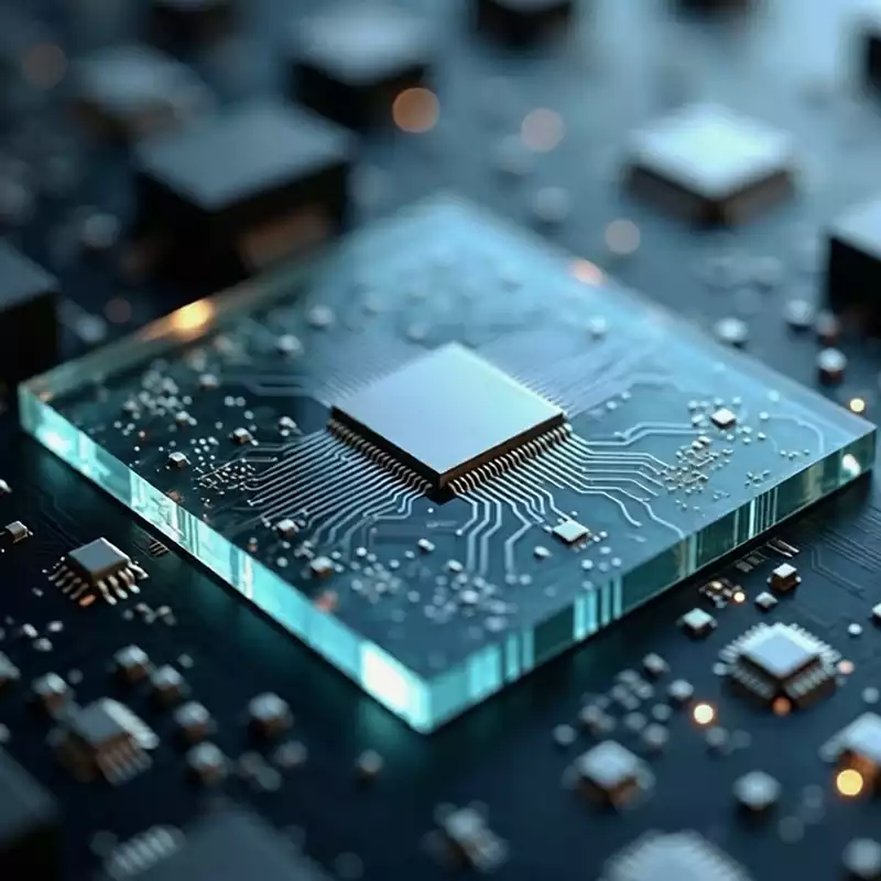
What is a glass substrate? A glass substrate is a circuit board that uses glass as its core substrate material. It has replaced the FR-4 epoxy glass fibre boards long used in the electronics industry, becoming the next-generation platform material for high-end packaging and advanced interconnects.
Compared to traditional organic substrates, glass offers a range of unique advantages in terms of thermal performance, electrical properties, optical characteristics and mechanical strength. Consequently, in applications where signal integrity, thermal management efficiency and long-term reliability are of the utmost importance, glass substrates are rapidly becoming an indispensable choice.
Mainstream glass substrate materials and their characteristics
Fused silica glass is one of the most classic high-end substrate materials. It can withstand extreme temperatures of up to 1000°C, has an extremely low coefficient of thermal expansion, and possesses excellent optical transparency. For this reason, it is widely used in laser equipment, photolithography masks, and various high-precision instruments.
Microcrystalline glass is a composite material that combines the toughness of glass with the stability of ceramics. With its low dielectric constant and minimal signal transmission loss, it serves as a core material for ensuring signal stability in high-frequency equipment such as 5G base stations and radar systems.
Although sapphire glass is relatively expensive, it possesses exceptional resistance to chemical corrosion and excellent infrared transmittance, making it an indispensable key substrate in military infrared detection equipment and high-end optical instruments.
Tempered glass (chemically strengthened glass) excels in mechanical strength, with impact and vibration resistance far surpassing that of ordinary glass, making it highly suitable for applications demanding exceptional stability, such as rugged outdoor surveillance equipment and in-vehicle night vision devices.
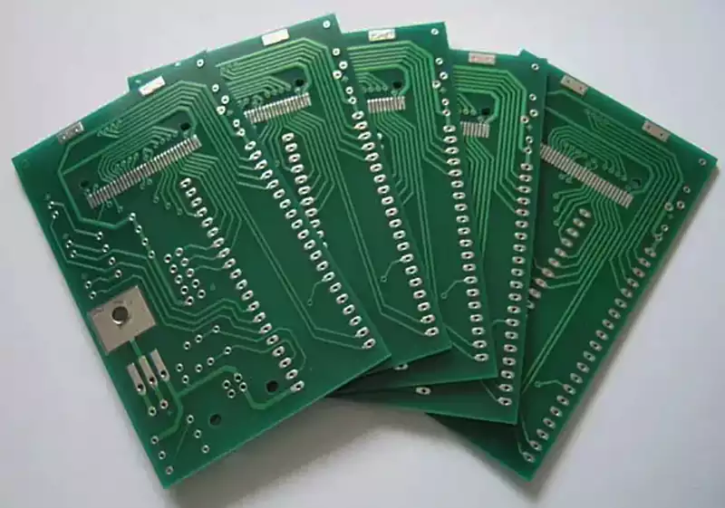
Although epoxy glass (i.e., FR-4) is strictly speaking an organic-inorganic composite substrate, its outstanding cost-effectiveness, moderate heat resistance and mature manufacturing processes make it the most widely shipped and applied ‘affordable’ solution within the glass substrate family, covering the vast majority of consumer electronics and general-purpose products.
It is worth noting that in recent years, alkali-free glass and borosilicate glass have also begun to enter the field of semiconductor packaging. Alkali-free glass contains no sodium ions, effectively preventing circuit parameter drift caused by ion migration; borosilicate glass, meanwhile, strikes a good balance between a low coefficient of thermal expansion and low cost, and is considered a potential candidate material for next-generation panel-level packaging.
Six Key Advantages of Glass Substrates Over Traditional Substrates
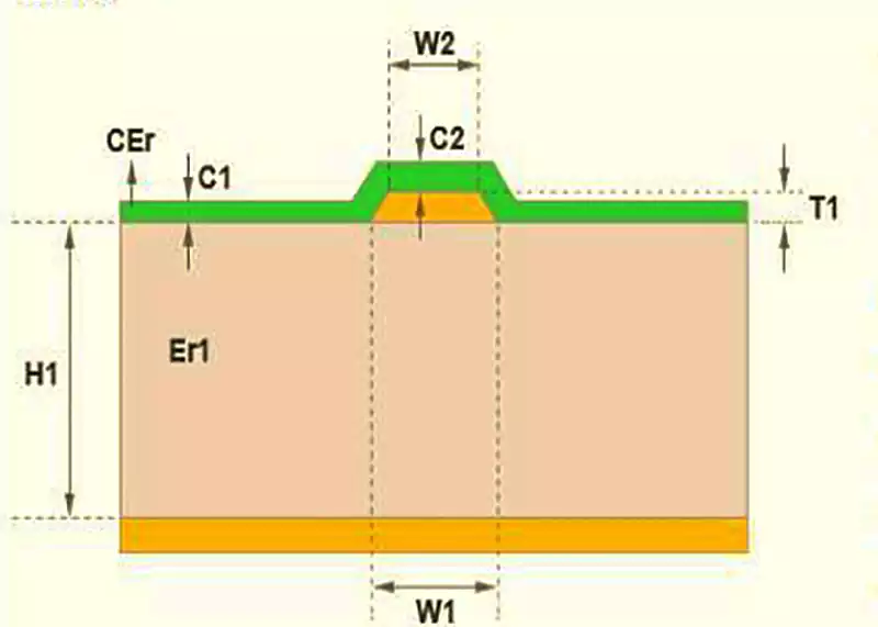
1.Ultra-high flatness and extremely low surface roughness. The surface roughness of glass substrates can typically be controlled to the sub-nanometre level, far surpassing that of organic substrates. This characteristic makes them an ideal platform for the manufacture of semiconductor devices with ultra-fine line widths and ultra-fine pitch, and is particularly suitable for RDL (re-wiring layer) processes in advanced packaging.
2.Exceptional thermal stability and a closely matched coefficient of thermal expansion. Glass substrates exhibit virtually no performance degradation under high-temperature conditions, and their coefficient of thermal expansion (CTE) is very close to that of silicon chips, at approximately 3.5 ppm/°C. This means that during chip mounting and reflow soldering, stress caused by thermal mismatch is significantly reduced, effectively preventing issues such as solder joint cracking and chip warping.
3.Superior dielectric properties. Certain glass materials possess a high and stable dielectric constant, which helps to reduce the physical dimensions of passive components such as capacitors and inductors, thereby enhancing overall integration density. Additionally, the tangent of the loss angle of glass substrates is extremely low, ensuring signal integrity even at GHz and millimetre-wave frequencies, which is crucial for high-speed digital circuits.
4.Outstanding chemical stability. Glass substrates exhibit strong resistance to moisture, acids, alkalis and organic solvents. In harsh environments such as high humidity and high salt fog, their performance degradation is far slower than that of organic substrates, providing longer-lasting protection for sensitive components within the package.
5.Optical transparency and tunable optical parameters. For packages requiring optical windows (such as image sensor packages and optical communication modules), the high transparency of glass substrates is unmatched by organic substrates. Furthermore, by doping with different elements, the refractive index of the glass can be precisely controlled, providing design flexibility for on-chip optical interconnects.
6.Environmental friendliness and exceptionally long lifespan. Glass substrates contain no volatile organic compounds (VOCs), making them more environmentally friendly during both manufacturing and use. Their inorganic nature ensures they do not age, yellow or degrade in performance over time, as organic materials do, with a theoretical lifespan of up to several decades.
Applications of Glass Substrates
High-speed digital circuits are one of the most representative applications of glass substrates. In scenarios requiring multi-GHz frequencies, such as AI accelerators, data centre switches and high-end routers, glass substrates enable distortion-free signal transmission thanks to their extremely low dielectric loss.
High-power circuits also benefit from the properties of glass substrates. Their high thermal conductivity effectively dissipates heat generated by power devices, making them widely used in power electronics applications such as electric vehicle inverters, industrial frequency converters, and rail transport.
High-temperature electronic products represent another key area for glass substrates. Glass PCBs can operate continuously at temperatures exceeding 200°C without any degradation in performance, making them suitable for downhole oil and gas detection equipment, aerospace electronic systems, and control modules within automotive engine compartments.
High-frequency and millimetre-wave antennas demand exceptional stability in dielectric properties. Glass substrates maintain a stable dielectric constant and low loss even in the millimetre-wave band, making them highly suitable for applications such as 5G/6G base station antenna arrays, vehicle-mounted radar, and satellite communications.
Sensors and transducers leverage the glass substrate’s resistance to corrosion and moisture. Whether in gas sensors within chemical environments, pressure sensors in the deep sea, or MEMS inertial devices, glass substrates provide a reliable long-term operating environment.
Medical electronics is a rapidly growing sector. The durability and biocompatibility of glass substrates make them suitable for applications such as implantable neural stimulators, in-body monitoring devices and surgical robot control boards, allowing for long-term implantation in the human body without triggering an immune response.
In the field of AI chip packaging, glass substrates are emerging as a key material for ‘breaking through barriers’. As chip computing power approaches the physical limits of silicon-based interconnects, the industry urgently requires a substrate capable of supporting more layers of RDL and finer circuit patterns.
Thanks to their ultra-flat surfaces and low coefficient of thermal expansion, glass substrates are considered the most realistic path to achieving interconnect densities surpassing those of organic substrates.
The Complete Process for Manufacturing Glass Substrates
1.Material Preparation and Surface Treatment. The manufacturing process begins with a thorough cleaning of the glass substrate. Typically, an ultrasonic cleaner is first used to remove surface dust and debris, followed by chemical cleaning with organic solvents such as isopropyl alcohol (IPA), and finally rinsing with deionised water and drying. The sole purpose of this series of operations is to ensure that the subsequently deposited copper layer forms a strong chemical bond with the glass surface, rather than merely adhering physically.
2.Photolithography to Define the Circuit Pattern. A layer of photoresist is uniformly applied to the clean glass surface; this comes in two types: positive and negative. Positive photoresist is dissolved and removed in areas exposed to ultraviolet light, whilst negative photoresist hardens and remains in the exposed areas. The substrate is then aligned with the circuit design mask and exposed to ultraviolet light; after rinsing with a developer solution, a precise circuit pattern is left on the substrate.
3.Deposition of the conductive layer. The core task of this step is to ‘grow’ a layer of copper on the glass. Three methods are commonly used in the industry: magnetron sputtering involves bombarding a copper target in a vacuum, depositing copper atoms onto the glass surface; whilst chemical vapour deposition (CVD) utilises gaseous precursors to react on the substrate surface and form a copper film, making it suitable for large-area, uniform coverage.
Electroless copper plating (chemical copper plating) requires no external current; it utilises a chemical reaction to self-catalyse the deposition of a copper layer on the substrate surface. This is the most commonly used method for glass substrates—as glass itself is non-conductive, an initial conductive layer must first be established via electroless plating.
4.Laser drilling and via fabrication. When the circuit design requires interlayer electrical connections, holes must be drilled in the glass substrate. As glass is hard and highly brittle, mechanical drills are highly likely to cause cracking; therefore, laser drilling has become the standard process. Commonly used lasers include ultraviolet picosecond lasers and femtosecond lasers; the former produces a small heat-affected zone and smooth hole walls, whilst the latter can process microvias of smaller diameters, down to tens of micrometres.
5.Surface finishing and protective coating. After circuit fabrication is complete, the substrate must undergo multi-layer protective treatment. Electrolytic nickel-gold (ENIG) deposits a dual nickel/gold layer in the pad areas, enhancing soldering reliability and oxidation resistance; the solder mask covers non-soldering areas to prevent short circuits and solder bridges; conformal coating, meanwhile, applies an ultra-thin protective film across the entire board surface, providing triple protection against moisture, dust and corrosion.
The Core Process of Glass Substrates – TGV (Through-Glass Via)
TGV (Through-Glass Via) is the hallmark technology that distinguishes glass substrates from all other substrates. It enables the creation of microscopic conductive vias within the glass, facilitating vertical electrical interconnections between chips and between chips and the substrate.
The complete TGV process is divided into two main stages: via formation and filling.
TGV Via Formation: Five Mainstream Technical Approaches
The sandblasting method creates vias by physically bombarding the glass with high-speed abrasive particles; it features simple equipment and low cost, but the via walls are rough and precision is poor.
The photoresist glass method utilises differential etching of photosensitive regions within the glass to create vias; it allows for batch processing but is limited in material selection.
Plasma etching utilises reactive ions to bombard the glass surface; it offers good anisotropy and high precision, but has a slow etching rate and is relatively expensive.
Laser ablation directly evaporates glass material using a laser to create holes; it is flexible and non-contact, but the heat-affected zone may cause micro-cracks.
Laser-induced wet etching (LIDE) is currently the most prominent technology. Its core principle is as follows: a pulsed laser is first used to induce a continuous denatured zone within the glass; the etching rate of this denatured zone in hydrofluoric acid (HF) solution is significantly higher than that of the undenatured regions. Based on this difference, the chemical solution follows the laser-induced path to ” “to form the through-hole.
As the process is primarily chemical etching with the laser merely acting as an initiator, the hole walls suffer almost no thermal damage, and the sidewall smoothness can reach the sub-micron level. This technology has been proven suitable for quartz glass, borosilicate glass and even flexible ultra-thin glass, and is considered a key enabling technology for the mass production of glass substrates.
TGV In-hole Filling: Metal Plating Solution
After hole formation, the interior of the through-hole is empty insulating glass, which must be filled with conductive material to achieve electrical connection.
The mainstream approach is metal electroplating filling, with the specific process as follows: first, an extremely thin titanium/copper seed layer is sputtered onto the inner wall of the through-hole to provide a conductive starting point for subsequent electroplating; then, via electrochemical deposition, copper ions gradually grow on the seed layer, eventually filling the entire through-hole.
In terms of filling strategies, there are two options: full filling and partial filling. Full filling offers the best electrical performance but is time-consuming, uses a large amount of copper and is costly. Partial filling (filling along the side walls of the via or using a semi-enclosed structure), however, has recently been proven to offer electrical performance virtually indistinguishable from full filling, whilst reducing process time by over 40% and copper consumption by over 30%; it has therefore become the mainstream choice for current industrial production.
Glass substrates are not intended to completely replace FR-4, but rather to establish an irreplaceable position in the high-performance, high-reliability, and high-density segments. From TGV via formation to RDL stacking, and from material selection to mass production processes, the entire technology chain is maturing rapidly.
The foreseeable trend is that between 2025 and 2027, glass substrates will first achieve small-scale mass production in AI accelerator packaging, 5G millimetre-wave modules and high-end sensors; from 2028 onwards, as the costs of LIDE via formation and partially filled TGV processes fall further, glass substrates are expected to enter the broader fields of high-performance computing and automotive electronics.