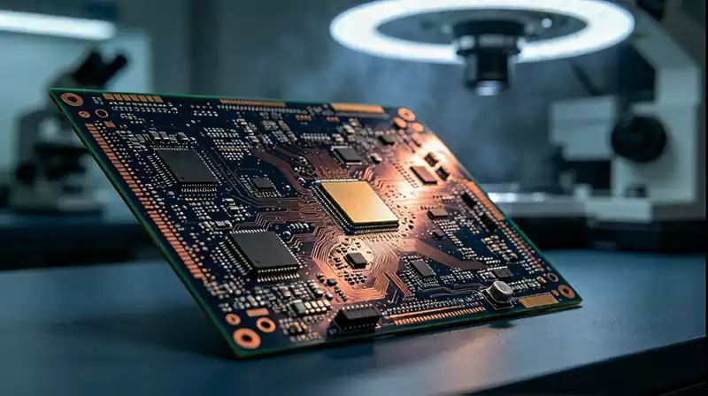
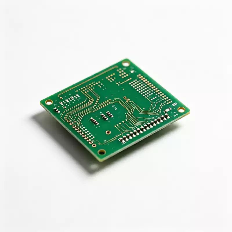
1 layer PCB, also known as single‑sided PCB, represents the most basic form of printed circuit board. Conductive copper foil exists only on one side of the dielectric substrate, and all circuit traces are arranged on this single conductive surface, while the opposite side retains pure insulating base material without any conductive paths.
After copper foil undergoes etching to form circuit patterns, partial copper areas are preserved for traces and soldering pads, and redundant copper is removed from the board surface. Solder mask ink is then applied to cover most conductive regions, exposing only pads for component soldering. In most assembly cases, components are inserted from the non‑conductive insulating side, with pins passing through drilled holes to make electrical contact on the copper‑clad side for soldering completion.
A typical 1 layer PCB is built with multiple stacked material layers. The base dielectric material widely adopted is FR‑4, while low‑cost mass‑production products often adopt phenolic paper‑based substrates such as FR‑1 and FR‑2. Copper foil with 35μm (1oz) thickness serves as the mainstream conductive layer bonded to one side of the substrate. Solder mask, available in green, black, red and other custom colours, protects traces from oxidation and short‑circuit risks. Silkscreen layer is printed on top to mark component identifiers, board revisions and other identification information. Paper‑based substrates deliver obvious cost advantages yet come with drawbacks including limited heat resistance and poor mechanical strength.
FR‑4 provides balanced insulation and thermal performance, making it suitable for simple power supply modules and general industrial control hardware.
Its manufacturing workflow is relatively concise compared with multi‑layer boards. The whole procedure starts from copper‑clad base material, followed by pattern transfer and etching, drilling, solder mask printing, silkscreen marking and final surface finish. Hot air solder levelling remains the dominant surface treatment option for mass orders. OSP antioxidant treatment is selected when further cost reduction is required. Gold immersion is rarely specified for 1 layer PCB projects, as this finish will significantly raise overall board cost.
Structural constraints define its practical boundaries. Since all traces are confined to one single conductive layer, circuit paths cannot cross each other without additional measures. Jumpers have to be introduced to resolve trace intersection conflicts. Excessive jumpers will increase assembly workload and reduce long‑term system reliability, so 1 layer PCB is only feasible for low‑complexity circuits.
It fits well for a wide range of mature consumer hardware, including simple power adapters, remote controller boards, home appliance keypad control units, toy circuits and low‑power LED lighting assemblies where signals run at low speed and component quantity stays limited. This board type is not recommended for high‑speed or high‑frequency circuits, high‑component‑density hardware, systems with numerous intersecting signal lines, and devices requiring dedicated grounding shielding. For these demanding scenarios, double‑layer or multi‑layer PCB is the more reasonable choice.
Designers need to take manufacturing feasibility fully into account during schematic and layout work. Trace crossing conflicts shall be anticipated at early layout stages, and proper pad positions for jumpers should be pre‑reserved instead of being handled in post‑production modification. For FR‑4 material with 1oz copper foil, trace width and spacing above 0.2 mm delivers stable yield for mass production, though 0.15 mm can be accepted as the technical limit for small‑batch prototyping. For through‑hole components, drilled hole diameter should be 0.2‑0.3 mm larger than component pin size. Special attention should be paid to paper‑based boards, whose substrate tends to fuzz during drilling and cannot sustain frequent mechanical bending.
From the cost perspective, 1 layer PCB brings obvious price benefits thanks to fewer material inputs and simplified processing steps for both prototype and volume orders. When circuit complexity grows to demand large amounts of jumpers, extra material and manual soldering expenses will accumulate. Under such circumstances, total comprehensive cost can approach double‑layer PCB, so upgrading to double‑layer boards becomes more economical.