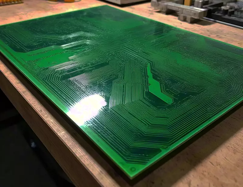
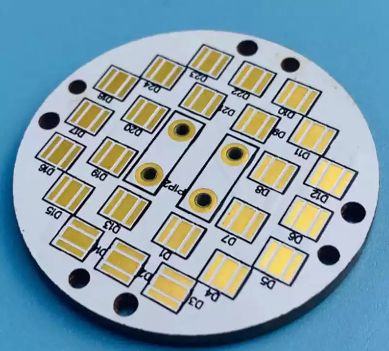
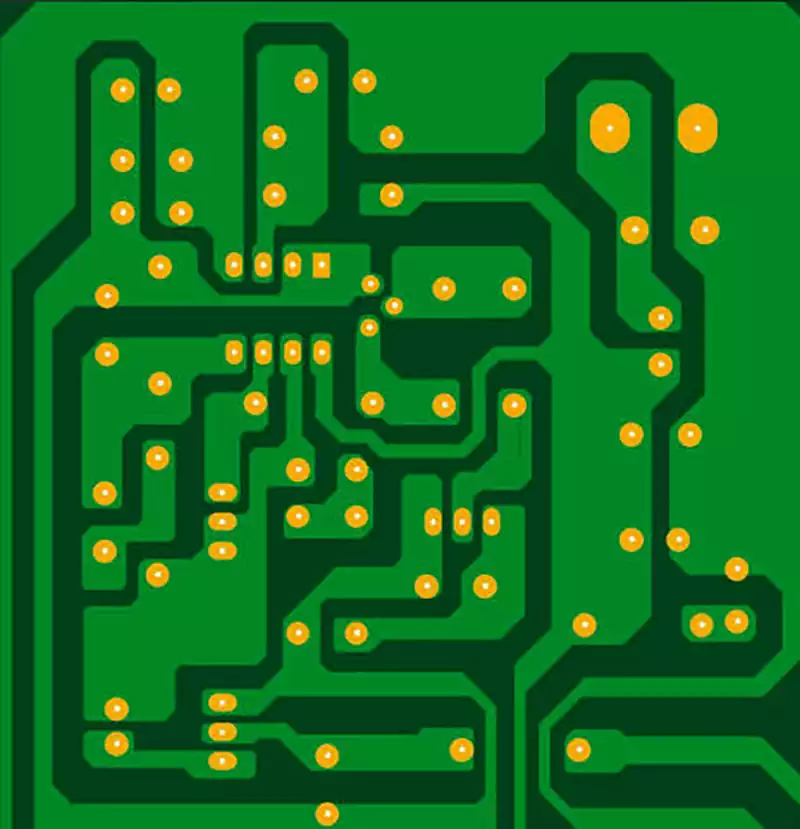
Bare PCB testing verifies that every net on a fabricated board conducts as designed and that separate nets remain insulated from one another. It catches opens and shorts that visual inspection cannot reveal. Once copper patterning and etching are complete, only electrical measurement can confirm whether the foil connects as designed; visual examination cannot replace it.
Two types of equipment dominate bare PCB testing. Bed-of-nails systems use fixed probes that contact all test points at once, while flying probe systems use a small number of moving probes that visit points in sequence. The choice depends on production volume, how often the board type changes, and the condition of the test points on the board.
What bare PCB testing detects
Bare PCB testing determines two states. Continuity within a net corresponds to an open circuit, insulation between nets corresponds to a short, and neither involves component parameters because testing takes place before assembly. Engineers commonly group inspection into three stages: bare board inspection, in-circuit inspection after assembly, and functional testing. Bare PCB testing occupies the first stage, with the aim of stopping inherent continuity defects before assembly begins. Once assembly places components on a multilayer board, inner-layer conductors become difficult to rework, so moving the test earlier gives the most direct benefit.
Resistance and capacitance methods in bare PCB testing
Bare PCB testing judges continuity by measuring electrical quantities on each net. The resistance method assigns a threshold to the net under test. Resistance between two endpoints above the open threshold indicates an open circuit, and resistance between separate nets below the insulation threshold indicates a short. Test programs commonly set the insulation resistance threshold at 20 megohms.
The capacitance method treats the board surface and a reference plane as the two plates of a capacitor, since changes in conductive pattern area alter the capacitance reading. When all endpoints on one net give equal capacitance, a lower reading at one endpoint indicates an open, and converging readings from two nets suggest a possible short. The capacitance method runs quickly, but associated capacitance and secondary capacitance affect its readings, which makes it less reliable than the resistance method for single-point nets in particular.
How bed-of-nails fixtures work in bare PCB testing
Bed-of-nails testing uses spring-loaded probes arranged on a fixed grid to contact test points simultaneously. The springs apply 100 to 200 grams of force per probe to maintain reliable contact. Universal grid handlers place pins at centre spacings of 100, 75, or 50 mil. When board pads sit on the grid, a single closure completes continuity checks on all nets.
A bed-of-nails fixture can measure several thousand test points at once, and a single-side test usually takes only tens of seconds, with test time rising little as net count grows. The cost is a dedicated fixture for every board type, along with expensive equipment that is difficult to repair. Bed-of-nails testing therefore suits high-volume production of fixed designs. Probe access also limits its reach: dense point locations call for higher-density fixtures.
How flying probe systems work in bare PCB testing
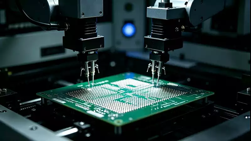
Flying probe testing does not rely on a probe pattern fixed in a fixture. Computer data drives four to eight independently moving probes on an X-Y mechanism, and these contact test pads and vias in sequence. Two probes can travel within 4 mil of each other, the minimum test gap can reach 0.2 millimetres, and positioning accuracy and repeatability reach 5 to 15 micrometres. These figures let flying probe systems reach fine nodes that bed-of-nails fixtures struggle to access.
The method needs no fixture, and changing board types requires only loading the corresponding program, which suits prototypes and low-to-medium volumes. Speed is the limitation. A board that a bed-of-nails fixture tests in tens of seconds may take a flying probe system eight to ten minutes or longer. The X-Y mechanism also caps board size, usually at 16 inches by 24 inches or less. Physical contact between probe and solder leaves small dimples. Some customers treat these as cosmetic defects, and soft-landing technology can reduce the effect.
Choosing between bed-of-nails and flying probe in bare PCB testing
The choice between bed-of-nails and flying probe depends mainly on production volume and how often board types change. Prototypes and fast-turn products use flying probe testing. Moving from data receipt to the start of testing takes only a few hours, which removes fixture development and waiting time. Boards with a fixed design and stable volume use bed-of-nails testing. High volume spreads the fixture cost across the batch, and per-board test cost can fall to two to four percent of the selling price. Test development time differs as well.
Engineers may spend several weeks building a bed-of-nails fixture, while they prepare a flying probe program in hours. For volumes between the two cases, a universal bed-of-nails fixture and a flying probe system can work together. The fixture handles production boards on a standard grid, and the flying probe system handles dense boards or designs subject to last-minute changes.
Coverage and netlist data in bare PCB testing
Coverage in bare PCB testing depends on whether the test checks every net, with full netlist testing as the ideal. A test program needs netlist data to define which endpoints should connect and which nets should stay isolated. An early industry standard, IPC-D-356, converts a CAD netlist into a format that test equipment can read, so reports can identify the connections of a specific net. Gerber machine code can also yield a netlist, but it carries no component information and describes only the conductive connections formed by photoplot commands.
Differences among the three electronic descriptions are common. They arise from rushed design changes, conversion problems between machine code and netlist, and software implementation faults. Inconsistent data leads directly to false calls or missed faults. As density rises, the physical limit of bed-of-nails fixtures becomes the coverage bottleneck. A four-density fixture holds 62 probes per square centimetre, while a ball grid array at 1.0 millimetre pitch has 96 connection pads per square centimetre. A bed-of-nails fixture cannot cover every point on such a board.
Grid constraints in bare PCB testing
The grid of a bed-of-nails fixture determines the equipment and also constrains test point design on the board. With a universal grid at 2.5 millimetre spacing, test pad diameter should be at least 1.3 millimetres. If the grid shrinks to 1 millimetre, pads need to exceed 0.7 millimetres. A grid that is too fine makes probes thinner, more brittle, and prone to damage, so engineers favour grids larger than 2.5 millimetres. Engineers have to consider this constraint during design. Where a test point misses the grid, pins cannot reach it, and the board needs flying probe testing or conductive rubber instead. Routing largely settles the choice of test method, and changing it later usually means relocating the layout.
Common questions about bare PCB testing
Can bare PCB testing replace in-circuit testing. No. Bare PCB testing checks copper continuity and net insulation before assembly, while in-circuit testing checks solder joints and component parameters after assembly. The two cover different defects at different stages.
Does a bare board that passes visual inspection still need electrical testing. Yes. Opens and shorts occur inside conductors, and visual inspection cannot identify them. Only electrical measurement confirms that each net conducts and that nets remain insulated from one another.
Can a bare board with test points off the grid use a bed-of-nails fixture. Engineers can use flying probe testing or conductive rubber instead. Flying probe systems move from point to point under data control, so a fixed grid does not limit them. Conductive rubber suits off-grid points, though uneven pad height after hot air solder leveling can affect contact.