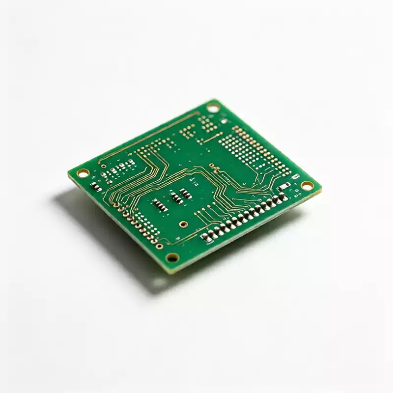
A PCB stackup defines the vertical structure of a printed circuit board and determines how copper layers and dielectric materials are arranged, separated, and laminated to form the finished board. For a multilayer PCB, the stackup specifies not only the sequence of signal, power, and ground layers, but also the thickness of the copper, the dielectric materials used between layers, and the final mechanical construction of the board.
At the beginning of a PCB project, the stackup may appear to be a simple technical specification. In reality, however, PCB stackup design is one of the most important decisions made during the entire PCB development process. The stackup establishes the electrical and mechanical foundation on which the rest of the PCB design is built.
A single product concept can often be implemented using dozens or even hundreds of possible PCB layer stackup configurations. However, only a limited number of these configurations can provide the required combination of signal integrity, controlled impedance, power integrity, electromagnetic compatibility, mechanical stability, thermal performance, and manufacturing cost.
A properly engineered PCB stackup provides high-speed signals with predictable return paths, creates suitable reference planes for impedance-controlled routing, helps reduce electromagnetic interference, and maintains sufficient mechanical balance during PCB lamination and thermal processing. An improperly designed stackup, on the other hand, can create signal integrity problems, impedance deviations, EMI issues, PCB warpage, and unnecessary manufacturing costs that are difficult to correct after the layout has been completed.
This guide explains what a PCB stackup is, how its individual layers and materials work together, how stackup design affects signal integrity and controlled impedance, and how to select an appropriate layer configuration for 2-layer, 4-layer, 6-layer, 8-layer, and higher-layer-count PCBs.
What Is a PCB Stackup?
A PCB stackup is the planned sequence of conductive copper layers and insulating dielectric layers that make up a printed circuit board. The stackup is normally determined before PCB routing begins because the position of each signal layer relative to its reference plane directly affects signal integrity, transmission-line impedance, and electromagnetic performance.
In a multilayer PCB, signal layers are used to route electrical connections, while ground planes and power planes provide reference structures and distribute electrical power. These conductive layers are separated by dielectric materials that provide both electrical isolation and mechanical support.
The two primary dielectric structures used in conventional multilayer PCB manufacturing are core and prepreg. A core is a rigid laminate with copper foil already bonded to one or both sides. It provides mechanical strength and establishes a controlled dielectric thickness between copper layers. Prepreg, short for pre-impregnated material, consists of fiberglass reinforcement impregnated with resin. During the lamination process, heat and pressure cause the resin to soften and flow, filling the spaces between the layers and bonding the entire multilayer structure together.
Once the lamination process is complete, the individual copper layers, cores, and prepreg layers become a single rigid PCB. Therefore, the PCB stackup determines much more than the physical order of the layers. It establishes the basic conditions required for controlled impedance, signal return paths, power distribution, electromagnetic performance, thermal management, and mechanical stability.
For this reason, PCB stackup design should be considered an electrical, mechanical, and manufacturing engineering task rather than simply a layer-ordering exercise.
The Five Fundamental Elements of a PCB Stackup
Signal Layers
Signal layers are the copper layers used to route electrical signals between components. Signals routed on the outer surfaces of a PCB typically form microstrip transmission lines, while signals routed between two reference planes form stripline transmission lines.
The transmission-line structure is determined by the relationship between the signal trace, the copper thickness, the dielectric material, and the adjacent reference plane. In general, an internal stripline structure provides stronger electromagnetic confinement because the signal is surrounded by reference planes. This can reduce electromagnetic radiation and improve isolation between high-speed signals.
For high-speed PCB designs, the position of each signal layer within the stackup is therefore extremely important. A signal layer should normally have a clearly defined and continuous reference plane nearby so that its return current can follow a short and predictable path.
Ground Planes
The ground plane provides a reference potential for the PCB and, more importantly for high-speed designs, provides a low-impedance return path for signal currents.
A continuous ground plane helps control the current loop area associated with high-speed signals, reducing unwanted electromagnetic radiation and limiting coupling between adjacent circuits. For this reason, maintaining ground-plane continuity is one of the most important principles of high-speed PCB stackup design.
When a high-speed signal is routed across a split, slot, or gap in its reference plane, the return current cannot follow its normal path directly beneath the trace. Instead, it must find an alternative path around the discontinuity. The resulting increase in loop area can contribute to higher EMI, increased crosstalk, signal distortion, and degraded eye-diagram performance.
Power Planes
Power planes distribute supply voltage throughout the PCB and can provide a low-impedance power-distribution structure when properly designed with adjacent ground planes.
When a power plane is placed close to a ground plane, the two conductive surfaces form a distributed capacitance. This plane-to-plane capacitance can help reduce high-frequency voltage fluctuations and improve the performance of the power distribution network (PDN).
The effectiveness of this structure depends on dielectric thickness, dielectric properties, plane geometry, current distribution, and the frequency range of interest. Therefore, power-ground plane coupling should be considered as one part of the overall power-integrity strategy rather than as a complete replacement for discrete decoupling capacitors.
Core Materials
The core is a rigid PCB laminate that typically contains fiberglass reinforcement and resin with copper foil laminated to one or both sides. In a multilayer PCB, the core contributes both mechanical strength and electrical insulation.
The thickness and dielectric properties of the core have a direct effect on controlled impedance because they determine the physical distance between signal traces and reference planes.
Prepreg
Prepreg is a fiberglass-reinforced material impregnated with partially cured resin. During PCB lamination, the resin flows under heat and pressure and bonds adjacent layers together.
The final thickness of the prepreg after lamination is particularly important for controlled-impedance PCB designs. Even relatively small changes in dielectric thickness can affect trace impedance, which is why the PCB manufacturer needs to account for the actual resin content, copper distribution, lamination pressure, and material characteristics when building the final stackup.
Copper Foil Thickness
Copper thickness is another critical parameter in PCB stackup design. Common copper weights include approximately 0.5 oz, 1 oz, 2 oz, and 3 oz copper, corresponding to approximately 17 μm, 35 μm, 70 μm, and 105 μm of copper thickness, respectively.
Thicker copper provides greater current-carrying capability and can be beneficial for power electronics and high-current applications. However, heavier copper also changes trace geometry and etching characteristics, which can affect controlled impedance and signal integrity.
For this reason, copper thickness should be established during stackup development rather than being selected after PCB routing has already been completed.
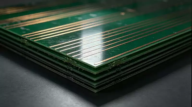
How PCB Stackup Design Affects Signal Integrity and EMI
Many signal integrity problems are initially attributed to routing geometry, but the underlying cause can often be traced to the PCB stackup itself. When a signal layer does not have an appropriate reference plane, the return current may be forced to follow an unpredictable path. This increases the electromagnetic loop area and can negatively affect both signal integrity and EMI performance.
One of the most important principles of high-speed PCB stackup design is to place each critical signal layer close to a continuous reference plane.
When a high-speed signal travels over a continuous reference plane, its return current tends to follow a path directly beneath the signal trace because this minimizes loop inductance. This creates a compact current loop and helps maintain predictable electrical behavior.
This relationship is especially important for controlled-impedance routing. The impedance calculated during PCB design assumes a specific relationship between the signal trace and its reference plane. If the physical stackup changes, the actual impedance can also change.
The situation becomes more problematic when a high-speed signal crosses a gap or split in the reference plane. Because the return current cannot cross the discontinuity directly, it must travel around the gap or find another return path. The resulting larger current loop can increase electromagnetic radiation and coupling while also contributing to signal distortion, jitter, and eye-diagram degradation.
Another important principle is to maintain appropriate spacing between power and ground planes. When the dielectric separating the two planes is relatively thin, the overlapping copper surfaces create significant distributed capacitance. For example, a power-ground pair separated by approximately 0.10 mm of dielectric can provide substantial plane capacitance over a large overlapping area.
This embedded capacitance can contribute to power integrity by reducing high-frequency impedance within the power distribution network. However, the actual effectiveness depends on the material system, plane size, geometry, and frequency range, so it should be evaluated together with conventional decoupling capacitors and the complete PDN design.
Controlled Impedance Depends on the PCB Stackup
Controlled impedance is fundamentally dependent on the PCB stackup. A PCB designer cannot establish a reliable impedance-controlled routing strategy without knowing the dielectric thickness, material properties, copper thickness, and reference-plane configuration.
The characteristic impedance of a PCB transmission line is influenced by several physical parameters, including trace width, copper thickness, dielectric constant (Dk), dielectric thickness, and the distance between the signal trace and its reference plane.
For example, if the reference plane is moved farther away from a signal trace, the characteristic impedance will change. Similarly, changing the prepreg thickness, laminate material, or copper thickness can alter the impedance even when the routing geometry remains unchanged.
This is why controlled-impedance requirements should be defined before PCB layout and routing begins. Attempting to correct impedance after the routing is complete can require significant changes to trace width, layer assignment, or even the entire PCB stackup.
Common impedance targets used in PCB design include 50 Ω single-ended transmission lines, 90 Ω differential pairs for USB interfaces, 100 Ω differential pairs for Ethernet and LVDS, and 85 Ω differential pairs for PCIe. DDR interfaces commonly use single-ended impedance targets within a range of approximately 40–60 Ω, depending on the specific memory interface, controller, PCB material system, and design requirements.
The required impedance tolerance also depends on the application and manufacturing capability. A general controlled-impedance PCB may use a tolerance of approximately ±10%, while more demanding high-speed applications may require ±5% or tighter tolerances.
Achieving tight impedance tolerances requires close control of PCB fabrication parameters, including copper etching, trace geometry, layer registration, dielectric thickness, prepreg resin flow, and lamination conditions.
The final manufactured PCB can be verified using appropriate test coupons and electrical measurement methods. Time-domain reflectometry (TDR) is commonly used for controlled-impedance verification when required by the PCB fabrication specification.
This explains why a PCB design can sometimes pass simulation but fail during laboratory testing. If the simulation uses an idealized stackup that differs from the actual manufactured construction, the simulated impedance and signal behavior may not accurately represent the finished PCB.
Common PCB Stackup Configurations for 2-Layer, 4-Layer, 6-Layer, and 8-Layer PCBs
Different PCB layer counts provide different combinations of routing capacity, reference planes, power distribution, electromagnetic isolation, and manufacturing complexity. The appropriate configuration depends on the electrical and mechanical requirements of the specific application.
2-Layer PCB Stackup
A typical two-layer PCB uses the following basic structure:
Top Signal / Bottom Signal
Two-layer PCBs provide a low-cost solution for relatively simple and low-speed circuits. Because there are no dedicated internal ground and power planes, however, high-speed signal return paths can be more difficult to control.
A two-layer PCB can still perform well when the circuit operates at relatively low speeds and the layout is carefully designed, but it becomes increasingly difficult to maintain controlled impedance and predictable return paths as signal speed and routing density increase.
4-Layer PCB Stackup
A commonly used four-layer configuration is:
Signal / Ground / Power / Signal
This is a widely adopted general-purpose multilayer PCB stackup because it provides dedicated internal reference and power planes while maintaining relatively low manufacturing cost.
A four-layer board can provide significantly better signal integrity and power distribution than a basic two-layer PCB, particularly when high-speed signals are routed on outer layers with appropriate ground references.
For certain high-speed applications, another configuration is:
Ground / Signal / Signal / Ground
This structure provides strong electromagnetic containment around the internal signal layers. Because the design does not include a dedicated internal power plane, however, power distribution must be implemented through other methods, such as copper pours or carefully designed power routing.
6-Layer PCB Stackup
A commonly used six-layer configuration is:
Signal / Ground / Signal / Power / Ground / Signal
Six-layer PCBs are frequently used for designs that include DDR memory, Ethernet, USB 3.x, PCIe, and other high-speed interfaces.
The additional layers provide more routing resources while allowing important signal layers to remain close to ground or power reference planes. With appropriate dielectric spacing and impedance control, a six-layer PCB can provide a practical balance between signal integrity, routing density, power integrity, and manufacturing cost.
8-Layer PCB Stackup
An eight-layer PCB provides additional routing and reference-plane resources and can accommodate more complex combinations of signal, power, and ground layers.
Eight-layer boards are commonly found in servers, high-speed networking equipment, automotive ADAS systems, RF and mixed-signal electronics, and other applications where electromagnetic compatibility and signal integrity are important design requirements.
The additional internal layers allow designers to create multiple stripline environments and separate different functional circuits more effectively. They also provide greater flexibility when allocating power and ground planes.
When the layer count increases beyond approximately eight layers, some applications begin to require HDI (High-Density Interconnect) technology. This is particularly common when fine-pitch components, high routing density, or severe space limitations make conventional through-hole vias impractical.
HDI designs may use microvias, blind vias, buried vias, and sequential lamination. As a result, the PCB manufacturing process and stackup design requirements become significantly more complex.
How to Choose the Right PCB Layer Count
PCB layer count should not be selected simply because a higher layer count appears more advanced. The objective of PCB stackup design is to use the minimum number of layers necessary to achieve the required electrical performance, routing density, power distribution, thermal performance, mechanical stability, and manufacturing reliability.
Three major factors should be evaluated when selecting the PCB layer count: routing density, signal speed, and power-distribution complexity.
For a relatively low-speed circuit with a simple component layout, a two-layer PCB may provide sufficient routing capacity and electrical performance.
For conventional digital electronics that require stable reference planes and controlled impedance, a four-layer PCB is often a practical choice.
When the design includes DDR memory, multiple high-speed serial interfaces, or higher routing density, a six-layer PCB can provide additional routing channels and reference planes that make high-speed layout considerably easier.
For servers, RF front-end modules, automotive ADAS systems, and complex mixed-signal equipment, an eight-layer or higher PCB may be appropriate when additional reference planes, routing resources, and electromagnetic isolation are required.
Two common mistakes should be avoided during layer-count selection.
The first is over-designing the PCB stackup by adding unnecessary layers. Extra layers increase material costs, board thickness, lamination complexity, registration requirements, and manufacturing risks. If the additional layers do not provide a meaningful electrical or mechanical benefit, they may simply increase project cost without improving performance.
The second mistake is under-designing the PCB stackup by forcing a high-speed circuit into an insufficient number of layers. This can lead to poor return paths, routing congestion, impedance-control problems, excessive crosstalk, and EMI issues.
For designs involving fine-pitch component fanout, microvias, or high-density interconnects, the stackup must also be developed together with the intended HDI manufacturing process.
Selecting the Right PCB Dielectric Material
The dielectric material used in a PCB stackup affects signal propagation, dielectric loss, impedance, thermal reliability, and manufacturing performance. Material selection should therefore be based on the electrical and mechanical requirements of the actual application rather than simply choosing the most expensive available material.
Standard FR-4
Standard FR-4 is widely used in conventional multilayer PCB manufacturing because it provides a good balance of electrical performance, mechanical reliability, availability, and cost.
Depending on the specific laminate, resin content, frequency, and measurement method, the dielectric constant, or Dk, of FR-4 materials is commonly within an approximate range of 4.2 to 4.6.
For many conventional digital, industrial, consumer, and mixed-signal applications, properly selected FR-4 materials can provide sufficient performance without the cost of specialized high-frequency laminates.
High-Tg FR-4
High-Tg FR-4 materials provide a higher glass transition temperature than standard materials. They are often selected for applications that require improved thermal reliability, especially when the PCB must withstand lead-free reflow soldering, multiple thermal cycles, or repeated lamination processes.
Low-Loss PCB Materials
Low-loss materials, including Rogers RO4003C and Megtron-series laminates, are commonly considered for high-speed digital, RF, and microwave applications where dielectric loss, Dk stability, and transmission-line performance become increasingly important.
At very high frequencies, particularly above approximately 10 GHz, low-profile copper can also be beneficial because copper surface roughness contributes to conductor loss as signal frequency increases.
Material selection should always be proportional to the actual electrical requirements. If a PCB operates only at frequencies in the lower hundreds of megahertz, using an expensive RF laminate may not provide a meaningful performance advantage and can unnecessarily increase material costs.
PCB Stackup Symmetry and Copper Balance for Preventing Warpage
Mechanical balance is another essential consideration in multilayer PCB stackup design.
A multilayer PCB should generally be constructed symmetrically around its mechanical centerline. The arrangement of copper layers, dielectric materials, and copper weights should be balanced as closely as practical on both sides of the center of the board.
For example, if one side of the stackup contains a large ground plane with a high copper percentage, the corresponding area on the opposite side should have a similar copper distribution whenever possible.
When copper distribution is significantly unbalanced, the different layers can experience different thermal expansion and contraction during lamination and subsequent thermal processing. This can contribute to PCB warpage or twisting and may eventually create assembly problems such as soldering defects, mechanical fit issues, or solder-joint reliability concerns.
A symmetrical PCB stackup is therefore one of the simplest and most cost-effective ways to reduce the risk of board warpage.
Balanced copper distribution also helps maintain more consistent dielectric thickness during lamination. Because dielectric thickness is an important parameter in controlled-impedance design, maintaining a stable and balanced construction can contribute to more predictable impedance performance.
When the PCB incorporates microvias, sequential lamination, or other HDI structures, the stackup must also satisfy the corresponding manufacturing and reliability requirements.
PCB Stackup Planning Should Be Completed Early in the Design Process
A PCB stackup should be established before the layout is finalized because many later design decisions depend directly on the stackup.
Once the total layer count, material system, copper thickness, dielectric thickness, reference planes, and impedance targets have been defined, these parameters influence component placement, fanout strategy, signal routing, return-current paths, power-plane allocation, thermal performance, manufacturing cost, and PCB fabrication yield.
A defective stackup cannot always be corrected simply by changing the routing.
For example, if a high-speed signal layer is positioned too far from its reference plane, changing the trace path may not solve the underlying impedance and return-path problem. Similarly, if the layer count is insufficient for the required routing density, no amount of minor routing optimization can fully compensate for the lack of available routing resources.
This is why PCB stackup planning should begin before detailed PCB layout and should be reviewed with the PCB manufacturer while the design is still relatively easy to modify.
Recommended PCB Stackup Design Workflow
A practical PCB stackup design process should begin by determining the required total layer count based on routing density, signal speed, power requirements, thermal conditions, and mechanical constraints.
The next step is to select the appropriate PCB material system and define the required ground and power-plane architecture. Once the reference-plane structure has been established, controlled-impedance requirements should be defined before high-speed routing begins.
The PCB designer and manufacturer should then work together to determine the appropriate dielectric thickness, copper thickness, trace width, spacing, and material construction required to achieve the target impedance.
Before the PCB layout is finalized, it is highly recommended to conduct a DFM (Design for Manufacturing) review with the PCB manufacturer. The manufacturer can evaluate whether the proposed stackup is compatible with available laminate materials, prepreg constructions, copper weights, lamination processes, registration capabilities, and controlled-impedance requirements.
The final stackup should then be documented as part of the PCB fabrication specification so that the manufacturer can build the board according to the approved construction.
A properly engineered PCB stackup provides the foundation for reliable signal integrity, controlled impedance, power integrity, EMI/EMC performance, thermal management, mechanical stability, and predictable PCB manufacturing.
The purpose of stackup design is not simply to determine how many copper layers a PCB should contain. A good multilayer PCB stackup establishes the correct relationship between signal layers, reference planes, dielectric materials, copper thicknesses, and mechanical structures so that the electrical and manufacturing requirements of the product can be achieved simultaneously.The key principles are straightforward: select the appropriate number of PCB layers, provide continuous reference planes for high-speed signals, define controlled impedance before routing, select dielectric materials according to the actual operating requirements, maintain symmetrical construction and balanced copper distribution, and involve the PCB manufacturer in DFM and stackup validation at an early stage.