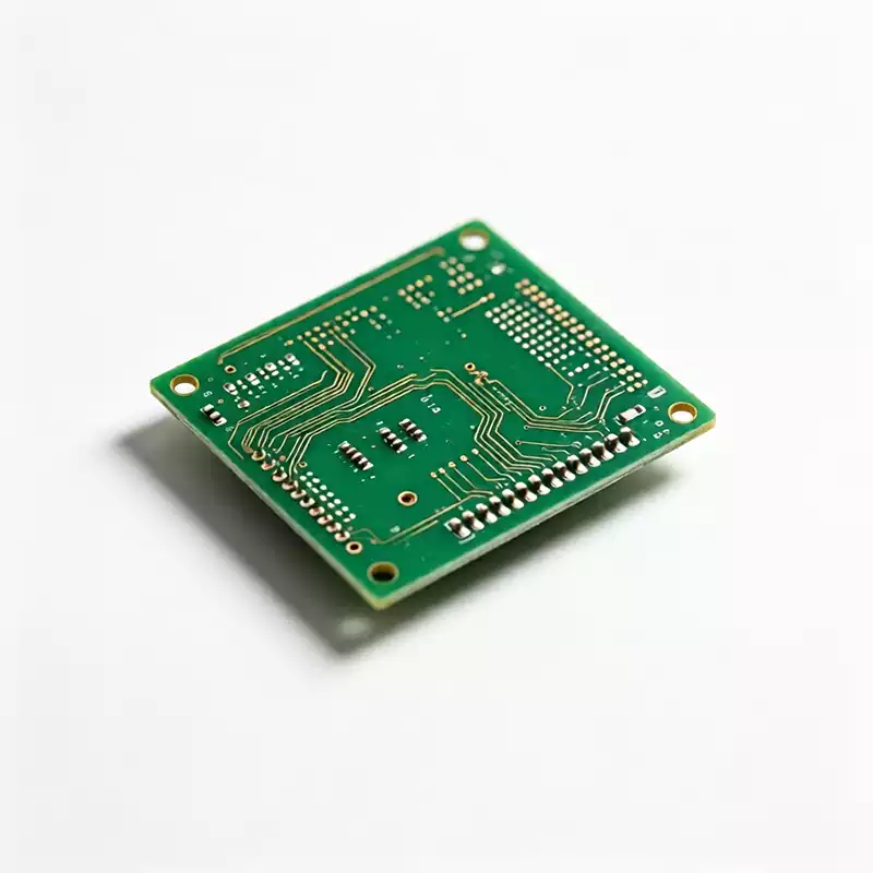
PCB board fabrication is the set of manufacturing steps that turns a digital design package into a bare, unpopulated printed circuit board. It is the part of the supply chain that builds the fibreglass-and-copper substrate itself, before a single component is placed. A PCB board that looks simple on screen can pass through more than a dozen tightly controlled chemical and mechanical operations before it is ready for assembly, and each one of those operations is where real yield, cost, and reliability are won or lost. This guide walks the full flow so you can read a fabrication drawing, brief a supplier, and judge whether a quoted process actually matches your design.
Differences Between PCB Board Fabrication and Assembly
The term “PCB board” can mean two different things, and confusing them is the single most common source of misquotes. Fabrication produces the bare board — copper traces, drilled holes, solder mask, and surface finish, but no parts. PCB board assembly (often written PCBA) comes afterwards and mounts components onto that bare pcb board. When you ask a shop for “PCB board fabrication,” you are asking for the blank board only; if you also need it stuffed, that is a separate assembly order with its own files, stencil, and test plan. Keeping the two steps distinct also keeps accountability clear: a short circuit found in test is a fabrication defect, while a tombstoned resistor is an assembly one.
Front-end engineering and the DFM review
Every pcb board starts as data, not as a physical object. Designers export Gerber files (or the smarter, self-contained ODB++ and IPC-2581 formats), NC drill and rout files, a fabrication drawing, and a stack-up note. Before any copper is cut, a CAM engineer runs a Design-for-Manufacturability (DFM) review against IPC rules and the shop’s own capabilities: trace width and spacing, annular ring, drill size, solder-mask clearance, copper-to-edge distance, and — for any high-speed net — controlled-impedance requirements. Problems caught here are cheap to fix; the same problem found after lamination can scrap the whole panel. A good PCB design handoff already anticipates these checks, which is why front-end engineering is where manufacturability is really decided.
Material selection and panel cutting
The base material is almost always a copper-clad laminate (CCL). Standard builds use FR-4, but RF, microwave, and many automotive or aerospace designs call for low-loss laminates such as Rogers where dielectric loss and Dk stability matter more than price. After the laminate is chosen, the large CCL sheet is cut into production panels sized to fit several boards plus tooling rails.
Panelization is rarely one board at a time; fabs pack multiple copies of your design — sometimes mixed with others — onto a single panel to spread setup cost and raise throughput. The material decision here is not a line item you fill in later: it sets the dielectric constant, the glass-transition temperature, and the loss tangent that every downstream electrical spec depends on. For the broader trade-offs, the advantages of FR-4 substrates and the case for Rogers in high-frequency work cover where each material earns its place.
Inner-layer imaging and etching
For any board with more than two layers, the internal circuitry is built first. Each inner core is cleaned, coated with liquid or dry-film photoresist, and exposed through the Gerber pattern so the circuit image transfers onto the resist. Unexposed or developed-away areas are then etched away in an acid bath, leaving only the wanted copper traces and pads. Etch time and chemistry concentration are controlled closely, because over-etching narrows conductors and under-etching leaves shorts. Every inner layer is then inspected — typically by automated optical inspection (AOI) — before it is allowed anywhere near the laminate press.
PCB Board Lamination Process
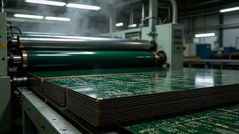
Lamination is the step that turns separate imaged layers into a single rigid body. The inner layers are stacked in the exact order specified by the stack-up, interleaved with prepreg (resin-soaked glass) and outer copper foil, then bonded under heat, pressure, and vacuum. Precise alignment is not optional: a few thousandths of an inch of layer shift can misregister a via and break a connection. This is also where symmetry matters — copper weight and layer order must mirror about the centreline, or the panel bows after thermal cycling. For a standard multilayer PCB the lamination is a single press cycle; HDI boards instead use sequential lamination, adding layers in repeated cycles, which is the heart of the modern HDI manufacturing process.
Mechanical and Laser Drilling
Holes are what connect the layers electrically, and they come in several flavours: through-holes that span the whole board, blind and buried vias that connect only some layers, and the laser-formed microvias used in dense HDI. Standard holes are drilled by high-speed CNC machines that can punch thousands of holes per panel; the smallest, highest-density features are cut by UV or CO₂ lasers because mechanical bits simply cannot reach them.
Registration between the drill file and the imaged layers is verified before the panel moves on. The reliability of these interconnects is governed by aspect ratio and by how cleanly the hole walls are prepared, which leads directly to the next step. The microvia classification and design guidelines spell out the rules different via types have to satisfy.
Hole metallization and copper plating
A drilled hole is just a hole in insulation until it is made conductive. The panel first goes through a cleaning and desmear step that removes resin smear from the hole walls, then an electroless copper deposition lays down a thin, uniform seed layer. Electrolytic copper plating follows to build the wall up to full thickness, turning every via and through-hole into a reliable electrical path between layers. This plating also adds copper to the outer surfaces, which is why outer-layer patterning has to be done afterwards rather than before.
Outer-layer imaging and pattern plating
With the panel drilled and plated, the two outer copper surfaces are imaged just like the inner layers: photoresist applied, exposed to the pattern, developed, and then plated where traces and pads must remain. The resist is stripped and the exposed unwanted copper is etched away, leaving the final external circuitry, including the pads that components will later solder to. Because the plating step adds to the defined pattern, etch compensation is built into the CAM data so the finished trace widths still meet the drawn specification.
Solder mask, silkscreen, and surface finish
Three coatings close out the bare board. A solder mask — green by default, though black, blue, and red are common — is applied and imaged over everything except the pads, protecting copper from oxidation and preventing solder bridges during assembly. Silkscreen ink then prints component outlines, polarity marks, and reference designators to guide placement and rework. Finally a surface finish protects the exposed pads: HASL is the economical default, OSP is thin and lead-free, and ENIG (electroless nickel immersion gold) dominates fine-pitch and high-reliability work because of its flatness and shelf life. The finish you pick has to match both your assembly process and how long the bare board will sit before it is populated.
Electrical test and final inspection
No board ships on trust. Each unit is electrically tested — by flying-probe for prototypes and low volume, or by bed-of-nails fixtures for production — against the netlist to catch opens and shorts. Automated optical inspection and dimensional checks confirm solder-mask registration, hole quality, and outline accuracy. For controlled-impedance designs, test coupons built on the same panel are measured with a time-domain reflectometer to verify the traces actually hit their target ohms. Only after these gates pass is the board routed or V-scored out of the panel and packed, usually in ESD-safe, moisture-controlled packaging with traceability records.
What drives lead time
Fabrication lead time tracks complexity. A standard 2–4 layer board typically runs 3–5 business days, a multilayer board 5–15, an HDI build 1–3 weeks, and rigid-flex longer still. Material availability, test requirements, and order volume move those numbers, but the biggest lever is how much of the flow is custom: more lamination cycles, more laser work, and tighter tolerances all add calendar days. Knowing this up front lets you trade a marginally cheaper stack-up for a week of schedule when the project is behind.
How to brief suppliers for successful PCB board fabrication
Getting PCB board fabrication right is less about watching the machines and more about giving the shop an unambiguous spec: a complete Gerber or ODB++ set, a fabrication drawing with class and tolerance call-outs, a clear stack-up, and your impedance and finish requirements stated explicitly rather than implied. Bring the fabricator in while the design is still cheap to change, ask for the DFM report, and confirm which IPC class you are building to before the first panel is cut. A board that starts with a precise, reviewable package is quieter, flatter, and far cheaper to produce than one rescued by exceptions and re-spins — and it is the difference between a fabrication order that ships on the date you were quoted and one that slips while the line waits.