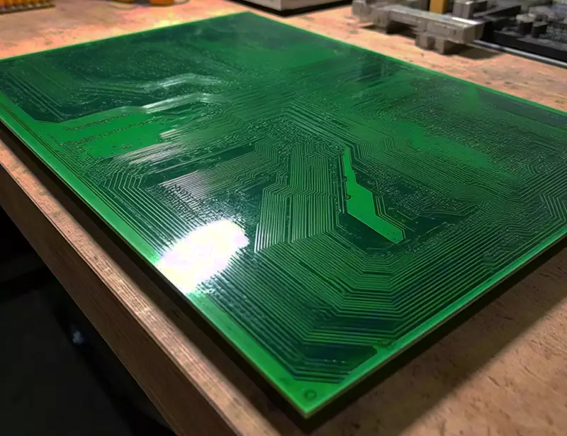
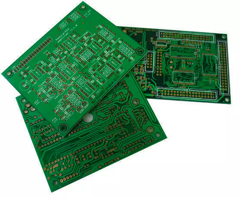
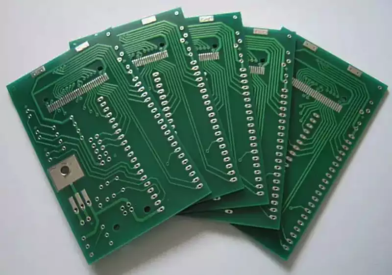
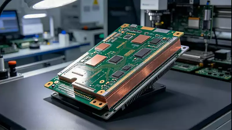
A printed circuit board (PCB) is the physical foundation of an electronic circuit. It supports components in defined locations and provides the electrical paths that connect them through copper traces, pads, planes and plated vias. Beneath those visible features is a carefully designed material and layer structure that determines how the board can be routed, assembled and operated.
A PCB board specification therefore involves much more than board dimensions or layer count. Copper thickness, dielectric materials, hole construction, surface finish and manufacturing tolerances all have to work with the electrical and mechanical requirements of the finished product. Small differences in these details can affect routing space, assembly compatibility, signal performance and production yield.
What Is a Printed Circuit Board?
A printed circuit board is an insulating substrate with a patterned conductive network used to connect electronic components. Copper is the most common conductor, while the dielectric material provides mechanical support and electrical separation between conductive layers.
The basic construction can range from a single copper layer to multiple copper layers laminated together. Single-sided and double-sided boards are relatively straightforward, while multilayer boards introduce internal signal layers, power planes and ground planes within the board structure.
The term PCB normally refers to the fabricated bare board. Once components are mounted and soldered onto it, the result is a printed circuit board assembly (PCBA). The distinction is important when preparing a quotation because bare-board fabrication and electronic assembly require different production data, processes and inspection criteria.
A PCB also forms part of the mechanical structure of an electronic product. Board dimensions, mounting holes, cutouts, edge features and connector locations must correspond with the enclosure and surrounding components. At the same time, trace geometry and the relationship between signal layers and reference planes influence signal propagation, return paths and power distribution.
Main Parts of a Printed Circuit Board
Substrate and dielectric materials
The substrate provides mechanical support for the copper circuitry and separates conductive layers from one another. FR-4, a glass-fiber-reinforced epoxy laminate, is widely used for rigid printed circuit boards because it offers a practical combination of electrical, mechanical and thermal properties.
Other constructions are used where standard FR-4 does not meet the application requirements. Flexible circuits commonly use polyimide, while metal-core boards can provide a more direct thermal path. Ceramic substrates and specialized high-frequency laminates are also used in applications with demanding electrical or thermal characteristics.
Important material properties include dielectric constant, dissipation factor, thermal stability, moisture resistance and mechanical strength. In high-speed and RF designs, the consistency of the dielectric properties becomes particularly important because changes in dielectric behavior can affect impedance and signal propagation.
Copper traces, pads and planes
Copper traces form the conductive paths between component connection points. Pads provide the areas where component leads, terminals or other conductive structures are soldered. Larger copper regions can function as ground or power planes, distributing current while also providing reference structures for signal routing.
Trace width and copper thickness are closely related to current capacity and fabrication requirements. High-current circuits may require wider conductors or heavier copper, while high-speed interfaces often require controlled trace geometry, appropriate spacing and a stable reference plane.
These dimensions cannot be considered independently. Increasing copper thickness, for example, can affect etching characteristics and minimum feature sizes, while changing dielectric thickness can alter impedance. The board construction has to support both the electrical target and the fabrication process.
Vias and plated holes
Vias provide electrical connections between conductive layers. A conventional through-hole via extends through the board, while blind and buried vias connect selected layers within a multilayer structure.
Via construction has a direct effect on routing flexibility. Through-hole vias are suitable for many conventional designs, but they consume routing space across multiple layers. Blind vias can connect an outer layer to an internal layer without passing through the entire board, while buried vias remain within the internal structure.
Dense layouts, fine-pitch packages and HDI designs may require microvias or via-in-pad structures. These technologies can create additional routing space, but they also introduce tighter manufacturing requirements and more complex fabrication steps. The via strategy is therefore best established early in the PCB design rather than treated as a late-stage layout adjustment.
Solder mask and legend
The solder mask covers most exposed copper while leaving selected pads open for soldering. Besides protecting the copper surface, it helps reduce the likelihood of solder bridging between closely spaced conductive features.
The legend, often referred to as silkscreen, provides visual information such as reference designators, polarity indicators, component markings and other assembly-related information.
Both layers are part of the manufacturing data. Pad openings, clearances and markings need to be defined accurately so that the finished board matches the intended assembly process.
Common Types of Printed Circuit Boards
Printed circuit boards can be categorized by layer count, mechanical construction, material system or interconnection technology. These classifications are not mutually exclusive. A board, for example, can be rigid, multilayer and HDI at the same time.
Single-sided PCBs
A single-sided PCB contains copper circuitry on one side of the insulating substrate. Its relatively simple construction makes it suitable for circuits with limited routing requirements, including some control electronics, lighting products and basic consumer devices.
The main limitation is routing area. Since conductive features are available on only one side, component placement and trace routing have to be planned carefully to avoid unnecessary crossings and layout constraints.
Double-sided PCBs
A double-sided PCB has conductive patterns on both sides of the substrate. Plated through-holes and vias provide connections between the two copper layers, giving designers considerably more routing flexibility than a single-sided board.
This construction is common in products that require more circuit density but do not justify the additional fabrication steps associated with internal layers. It can accommodate a broad range of electronic circuits while keeping the board structure relatively straightforward.
Multilayer PCBs
A multilayer PCB contains three or more conductive layers separated by dielectric materials and bonded into a single structure. Internal signal layers, power planes and ground planes provide additional routing capacity and allow designers to separate functions within a compact board.
Layer count, however, is only one part of the stackup. The location of signal and reference layers, dielectric thickness, copper weight and via structure all affect electrical behavior and fabrication requirements.
A well-planned multilayer stackup can provide controlled impedance, shorter return paths and better use of the available routing space. A poorly matched stackup can create unnecessary routing difficulty even when the total layer count appears sufficient.
Flexible and rigid-flex PCBs
Flexible PCBs use bendable dielectric materials to accommodate circuits that need to fold, bend or fit into irregular spaces. Rigid-flex PCBs combine rigid board sections with flexible interconnect areas, allowing several circuit regions to form one integrated assembly.
Mechanical behavior is a major part of the design. Bend radius, flex-layer construction, copper selection and the placement of components or vias near bending areas all need careful consideration. The intended bending direction, frequency of movement and assembly method should also be established before fabrication.
HDI and specialized PCBs
High-density interconnect (HDI) PCBs use fine-line structures and advanced interconnection technologies to accommodate dense component layouts. Depending on the construction, an HDI board may incorporate microvias, sequential lamination and via-in-pad technology.
These features are particularly useful around fine-pitch packages where conventional through-hole structures would consume too much routing space. They also require tighter control of drilling, registration, lamination and other fabrication parameters.
Other specialized PCB constructions address different engineering problems. Metal-core boards can be used where thermal dissipation is important, while RF and microwave laminates are selected when electrical behavior at higher frequencies becomes a primary design concern. High-current and demanding environmental applications may require additional material or construction considerations.
How Printed Circuit Boards Are Manufactured
The manufacturing sequence varies with the PCB board construction, but most boards pass through a series of related fabrication stages.
- Design data and engineering review
Production starts with the PCB fabrication package. Depending on the project, this may include Gerber or other manufacturing data, drill files, board outlines, stackup information and specifications covering material, finished thickness, copper weight, surface finish and tolerances.
The engineering review checks whether the supplied data is complete and internally consistent. Controlled-impedance requirements, unusual materials, specialized via structures and non-standard mechanical features should be clearly identified before fabrication begins.
- Inner-layer imaging and etching
For multilayer boards, the internal copper layers are patterned before lamination. Imaging transfers the circuit pattern to the copper-clad material, followed by etching to remove unwanted copper.
The resulting inner layers are inspected before they become part of the laminated structure. At this stage, defects or registration problems can be identified before additional fabrication steps make them more difficult to correct.
- Layup and lamination
The prepared cores, prepreg and copper foils are arranged according to the specified stackup. Heat and pressure then bond the individual layers into a single panel.
The lamination process determines the final relationship between conductive layers and dielectric materials. Layer alignment, material selection, pressing conditions and finished thickness all contribute to the dimensional and electrical characteristics of the completed board.
- Drilling and hole preparation
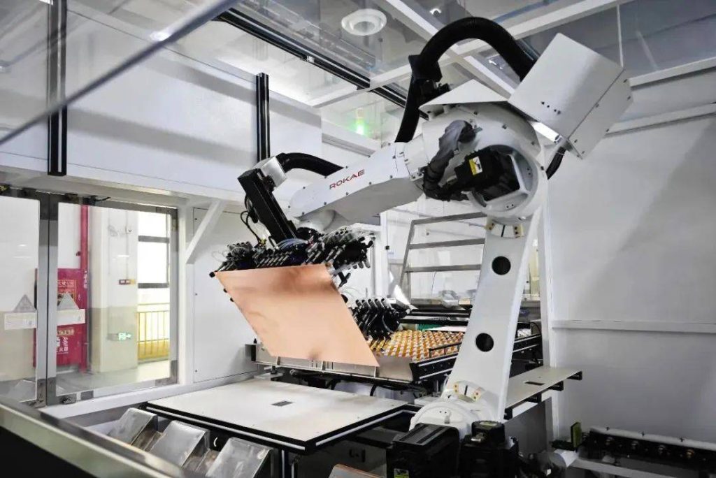
Drilling creates vias, plated through-holes and mechanical holes. Mechanical drilling is widely used for conventional holes, while laser drilling may be used for microvias and other fine interconnect structures.
Holes intended for electrical connections undergo preparation for copper plating. Non-plated mechanical holes follow a different process because they do not need an electrically conductive wall.
- Copper plating and outer-layer patterning
Copper is deposited onto the prepared hole walls to establish electrical connections between the required layers. The outer copper layers are then patterned to form the final traces and pads.
Conductor definition, plated-hole quality and interlayer continuity all require process control. These factors become increasingly important as trace widths decrease, aspect ratios increase or the board uses more complex interconnect structures.
- Solder mask, surface finish and legend
The solder mask is applied and patterned so that the required soldering areas remain exposed. A surface finish is then applied to exposed copper to protect the surface and provide the required solderability or contact characteristics.
Common surface-finish options include HASL, ENIG and other finishes selected according to the component technology, assembly process and application requirements. The legend is added where identification or assembly markings are required.
- Inspection and electrical testing
The finished boards are inspected against the applicable manufacturing and quality requirements. Depending on the product, inspection can include visual checks, dimensional verification, automated inspection and electrical testing for opens and shorts.
Additional verification may be required for boards with controlled impedance, specialized materials or other critical electrical characteristics.
The manufacturing route is not identical for every PCB. A simple single-sided board has a very different process flow from a high-density multilayer or HDI construction. The fabrication sequence should therefore be considered together with the actual board structure rather than treated as a fixed process for all PCBs.
What to Consider When Selecting a Printed Circuit Board
Electrical requirements: Define operating frequency, signal integrity targets, impedance requirements, current levels and isolation needs. These parameters influence trace geometry, reference-plane arrangement and, in some designs, laminate selection.
Mechanical constraints: Establish board dimensions, thickness, mounting holes, connector locations and mechanical loading. Products exposed to vibration, repeated movement or restricted installation space may require a different construction from a conventional rigid board.
Thermal conditions: Consider component power dissipation, ambient temperature and the available heat-transfer path. Copper distribution, substrate selection and specialized thermal constructions can all affect thermal performance.
Layer count and stackup: Determine the routing capacity required by the circuit, then consider how signal layers, ground planes, power planes, dielectric spacing and via structures should be arranged.
Assembly compatibility: Component footprints, pad geometry, surface finish, soldering method and panelization all affect the downstream assembly process. The bare-board design should be compatible with the intended SMT or through-hole assembly process.
Manufacturing tolerances: Review minimum trace width and spacing, hole diameter, annular ring, layer registration and other critical dimensions against the fabrication process being used.
Cost and production volume: Board cost is influenced by material selection, layer count, copper weight, via technology, process steps, yield and production volume. A lower layer count does not automatically produce the lowest overall manufacturing cost if it creates routing or fabrication difficulties.
What Information Should Be Included in a PCB circuit board Quote Request?
Fabrication data: Provide Gerber or other agreed manufacturing files, drill files and the board outline.
Board specifications: Include finished dimensions, board thickness, layer count, copper weights, material designation and surface finish.
Electrical requirements: Identify controlled-impedance requirements, electrical test requirements and any other characteristics that require verification.
Mechanical details: Specify slots, cutouts, edge plating, countersinks, mounting features, tolerances and other non-standard requirements.
Quantity and schedule: State prototype or production quantities, target delivery requirements and panelization information where applicable.
Special process notes: Identify HDI structures, sequential lamination, blind or buried vias, high-frequency laminates, heavy copper or other specialized construction requirements.
When a requirement is unclear, resolving it during engineering review is preferable to leaving the manufacturer to interpret the design intent. Clear documentation reduces the possibility of mismatched assumptions between design, fabrication and assembly.
Printed Circuit Board vs. PCB Assembly
A bare printed circuit board contains the substrate, copper circuitry, holes, surface finish and other fabricated features, but no electronic components. A printed circuit board assembly (PCBA) is created when components are placed and soldered onto the board.
The two manufacturing stages use different information. PCB fabrication focuses on the board structure, materials, copper features, holes, surface finish and dimensional requirements. Assembly requires additional information such as the bill of materials, component placement data, polarity, orientation, soldering requirements and inspection criteria.
When requesting a quotation, it is therefore useful to specify whether the project requires bare PCBs, PCB assembly or both. This keeps the manufacturing scope clear from the beginning.
Frequently Asked Questions
What does PCB stand for?
PCB stands for printed circuit board. It is the board structure that supports electronic components and connects them through patterned conductive features, most commonly copper.
What is the difference between a PCB and a PCBA?
A PCB is the fabricated bare board. A PCBA is the same type of board after electronic components have been mounted and soldered onto it. The terms refer to different stages of electronic manufacturing.
What materials are commonly used in printed circuit boards?
FR-4 is widely used for rigid PCBs, while polyimide is common in flexible circuits. High-frequency laminates, metal-core materials and ceramic substrates are used for applications with more specific electrical or thermal requirements.
How many layers can a printed circuit board have?
Printed circuit boards range from single-sided and double-sided constructions to multilayer designs with numerous internal conductive layers. The appropriate layer count is determined by routing density, circuit complexity, electrical requirements, mechanical constraints and the manufacturing process.
Why does PCB stackup matter?
The stackup defines how conductive and dielectric layers are arranged inside the board. It affects routing space, reference-plane placement, impedance, signal return paths, board thickness and fabrication requirements. For multilayer designs, stackup planning should be coordinated with both the electrical design and manufacturing process.
What files are needed to manufacture a PCB?
A typical fabrication package includes copper-layer artwork, drill data, the board outline and specifications covering material, dimensions, copper weights, surface finish and tolerances. Controlled-impedance boards, HDI constructions and other specialized designs may require additional documentation.
A printed circuit board is more than a substrate carrying copper traces. Its material system, layer structure, conductor geometry, via construction and manufacturing tolerances work together to determine how the board performs electrically and how reliably it can be fabricated.
The right printed circuit board construction starts with the requirements of the finished electronic product. Frequency, current, thermal conditions, mechanical constraints, component density and assembly requirements all contribute to the final board specification. Defining those requirements clearly during design and quotation gives the manufacturer a much clearer basis for reviewing the construction and selecting an appropriate fabrication process.