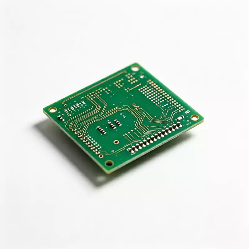
A rigid flex pcb is a special type of circuit board manufactured by integrally laminating rigid PCB regions and flexible PCB regions. The rigid areas use FR‑4 or high-Tg laminates for component mounting, while the flexible areas adopt polyimide (PI) films as substrates, capable of bending either during assembly or throughout the product service life. Compared with conventional multi-board wiring schemes that rely on cables and connectors, rigid flex pcbs eliminate harnesses and board-to-board connectors. Copper traces extend continuously from rigid sections through flexible regions to subsequent rigid segments, simplifying the mechanical structure and greatly improving vibration resistance and bending reliability.
This structure delivers three core advantages: removing connectors and solder joints — the primary mechanical failure points — to enhance shock and vibration tolerance; enabling 3D folded installation to fit compact and irregular enclosures; converting multi-component assembly challenges into standardized PCB manufacturing tasks for better batch consistency. A rigid flex pcb is not simply a rigid board attached with a flexible segment. It features an independent material system, dedicated design rules and industry standards, mainly governed by IPC‑2223 (design specification) and IPC‑6013 (qualification specification).
Structural Classification of rigid flex pcbs (IPC‑6013)
The industry categorizes flexible and rigid-flex circuits by stackup and fabrication process. Type 4 conventional rigid flex pcb is the most widely adopted variant in engineering practice.
Type 1: Single-sided flex circuit with coverlay on one side, for simple static interconnection
Type 2: Double-sided flex circuit with plated through-holes, supporting higher routing density
Type 3: Multilayer flex circuit, up to 4 conductive layers typically
Type 4 (Mainstream): Integrated structure combining multilayer rigid and flexible regions with plated through-holes. Max. 22 rigid layers and 10 flex layers
Asymmetric rigid flex pcb: Flex layers placed on outer surfaces for mixed-signal and shielding designs
HDI rigid flex pcb: Adopting buried and blind vias for high-density interconnection applications
For standard Type 4 rigid-flex boards, flex layers run through rigid zones as inner layers and remain unlaminated only in predefined bending windows so the flexible segments can deform freely, while rigid sections maintain sufficient strength for component soldering.
Main Stackup Configurations
The stackup of rigid flex pcbs directly affects board warpage, alignment accuracy and bending fatigue life. Three standard architectures are commonly used:
Symmetric stackup (Preferred): Copper and dielectric layers balanced about the central plane with copper distribution controlled within ±5%, effectively suppressing lamination warpage and registration offset
Asymmetric stackup: More layers on one side to thin the flex region at the cost of higher lamination complexity
Sandwich stackup: Flex layers enclosing internal rigid segments, mainly used for electromagnetic shielding and controlled impedance requirements
Core Material Selection Guidelines
Rigid flex pcbs incorporate two sets of material systems. Mismatch in coefficient of thermal expansion (CTE) between rigid and flexible materials is the root cause of most delamination and cracking failures.
1.Materials for Rigid Regions
FR‑4 or high-Tg FR‑4 laminates are commonly used with typical thickness ranging from 0.8 mm to 1.6 mm. Low-Dk laminates may replace standard materials for high-speed applications. Copper foil selection follows the rules for rigid PCBs.
2.Materials for Flexible Regions
Polyimide (PI) films of 25–50 μm thickness complying with IPC‑4202 are used for flex cores with ±10% thickness tolerance to guarantee impedance stability. Matching special copper foils are critical to bending fatigue performance.
3.Adhesives and Auxiliary Materials
No-flow or low-flow prepreg is applied in rigid areas, while acrylic or epoxy adhesive films are used for bonding flex layers. Key design rule: the thickness of acrylic adhesive within rigid sections shall not exceed 10% of the total board thickness to avoid reliability risks at plated holes caused by adhesive softening under reflow temperature.
Liquid solder mask shall not be used on flexible regions. PI coverlay must be applied for protection to prevent cracking during bending. Features such as ZIF connector fingers, shielding films and stiffeners can only meet IPC qualification via coverlay processes.
4.Stiffener Design
Local stiffeners are added underneath connectors, contact pads and components adjacent to flex zones. Available materials include PI, FR‑4 or stainless steel (max. 500 μm). Stiffeners convert local flexible areas into rigid support regions to prevent component solder joint fracture under stress.

Copper Foil Selection — Critical for Bending Life
Copper foil grain structure determines the fatigue resistance of flexible segments and represents one of the most error-prone design items. Foil type must be selected according to bending operating conditions:
RA Rolled Annealed Copper: Large-grain wrought structure with 20%–30% longer bending fatigue life, dedicated for dynamic repeated bending scenarios such as hinges and moving joints
High-elongation ED Electrodeposited Copper: Good ductility and cost-effective for static bending and mild dynamic flexure
Standard ED Electrodeposited Copper: Low ductility, only for one-time static assembly bending
Bending failure originates from copper fatigue crack propagation. Stress concentrates at trace corners, thickness transitions and pad entry points. RA copper is mandatory for products requiring long-term dynamic flexing and cannot be substituted.
Bending Radius Design Standards (Hard Thresholds)
Bending radius is the most critical quantified design parameter for rigid flex pcbs, calculated based on the inner surface of flex substrate. Large differences exist between static and dynamic requirements, which is a major cause of first-article failures.
Single-layer flex: Minimum bending radius ≥ 6 × flex thickness
Double-layer flex: Minimum bending radius = 10–12 × flex thickness
Multilayer flex: Minimum bending radius ≥ 24 × flex thickness
Dynamic continuous bending: 25–100 × total stack thickness
Static bending means deformation occurs only once during assembly and allows smaller radii. For structures subjected to continuous in-service flexing, the strict 100× thickness rule must be followed. Two special constructions are available for multilayer flex circuits requiring tight bending radii:
Bookbinder construction: Each flex layer is lengthened progressively toward the outer bend radius to eliminate compression and stretching during bending. Excellent performance but high cost and low yield
Air-gap construction: Flex layers remain unbonded across bending spans, with each layer bending around its own neutral axis. Simpler fabrication yet losing interlayer support within the flex region
Bending length must be calculated using formulas defined in IPC‑2223 instead of empirical estimation.
Zoned Design Specifications (Rigid / Bending / Transition Zones)
1.Routing Rules for Bending Zones
Route traces perpendicular to the bending axis. Parallel routing is forbidden to avoid stress concentration
No vias, plated through-holes or component pads in bending areas to prevent cracking at hole barrels or pad edges
All flex traces adopt curved routing; 90° sharp corners are prohibited
Traces on adjacent layers are staggered instead of stacked vertically, which would locally increase stiffness
Taper pad shapes at trace entry points to peel stress
2.Ground Plane Design for Flex Regions
Solid copper ground planes deliver optimal shielding but increase stiffness and degrade bendability. Hatched ground planes improve flexibility at the expense of reduced shielding performance and more complicated controlled impedance design, requiring trade-offs based on EMC requirements.
3.Transition Zones between Rigid and Flex Regions (High-Risk Areas)
The rigid-flex boundary features the highest stress gradient across the board and is prone to failure. Strict spacing rules apply:
Vias shall be at least 0.5 mm away from transition boundaries; ≥3.0 mm is recommended for high-precision products
Layer transitions are staggered by ≥1.5 mm to avoid abrupt stiffness change at a single cross-section
Use teardrop pads with increased annular ring size to enhance structural integrity
Vias placed above stiffeners are safe; vias right at stiffener edges carry maximum risk
Mass Production Process and Process Notes
Rigid flex pcbs cost more than ordinary PCBs mainly due to complicated sequential lamination and high-precision alignment. Standard manufacturing workflow:
Flex core preparation: LDI laser direct imaging is preferred to avoid damaging thermally sensitive PI films while maintaining high registration accuracy
Integrated lamination: Precisely position prepreg and adhesive films to prevent adhesive overflow into bending windows. Tooling fixtures compensate thermal expansion mismatch between rigid and flex materials
Drilling and plating: Combine mechanical drilling for through-holes and laser microvias for HDI structures to achieve uniform plating across rigid-flex interfaces
Controlled routing: Mill rigid outlines and cut bending windows precisely. Flex performance is released after depanelization
Stiffener/shield lamination and testing: Mount stiffeners and shielding films, followed by electrical tests, bend-cycle validation and thermal cycling reliability qualification
Reliability Qualification Standards (Industrial / Aerospace / Medical Grade)
High-reliability Class 3 rigid-flex boards must pass full quantitative reliability tests:
Thermal cycling: −55 ℃ ~ +125 ℃ to validate tolerance against CTE mismatch of stacked materials
Mechanical bending life: Minimum 100,000 cycles for dynamic applications; precision instruments may require over 500,000 cycles
Humidity insulation test: Insulation resistance ≥100 MΩ after 96 h conditioning at 40 ℃ and 93% RH
Plating requirement: Minimum copper thickness of 25 μm in plated through-hole barrels for Class 3 products
Most rigid-flex failures are not caused by defective materials but improper transition zone layout, insufficient bending radius or violated routing rules in flex regions.
Typical Applications
Space-constrained products: Mobile phones, wearables, cameras and hearing aids enabling 3D folded assembly
High-vibration environments: Automotive ADAS, vehicle sensors and robotic moving joints
Weight-sensitive systems: Avionics and satellite onboard equipment, reducing weight by eliminating harnesses and connectors
Long-term dynamic flexing: Notebook hinges, foldable displays and minimally invasive surgical instruments
Assembly simplification: Replacing multi-board harness assemblies with a single qualified PCB to reduce assembly errors and improve consistency
Cost Control and DFM Optimization Principles
Rigid flex pcb cost is determined mainly by flex layer count, special stackup types, copper foil grade, coverlay opening precision and reliability testing. Core mass-production cost-reduction strategies:
Minimize the number of flex layers and shorten flex segment length
Prioritize symmetric stackups to avoid rework risks from asymmetric structures
Avoid high-cost bookbinder construction unless tight bending radii are mandatory
Simplify coverlay openings and avoid fine features that reduce yield
Complete DFM review with manufacturers before layout finalization to prevent costly late design changes
By integrating rigid and flexible sections into one piece, rigid flex pcbs resolve pain points of traditional discrete PCB plus harness schemes including vibration-induced failure, packaging limitation and complicated assembly. Its design focuses on material matching, bending radius control, transition zone optimization and copper foil selection matching operating conditions. Compliance with IPC‑2223 / IPC‑6013 standards, adoption of symmetric stackups and standardized zoning routing ensures bending life and stable batch reliability, making rigid flex pcbs the core PCB solution for miniaturized, high-reliability electronic products with moving structures.