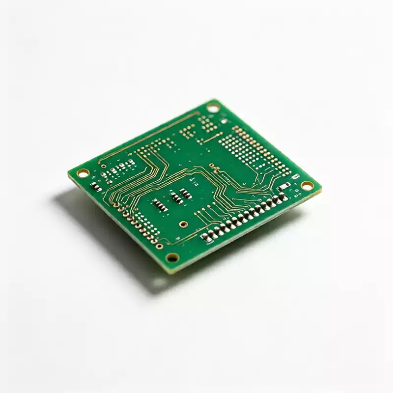
A microwave RF PCB is a specialized printed circuit board designed for high-frequency signal transmission. It serves as a critical component in advanced applications such as 5G communication infrastructure, satellite navigation, millimeter-wave radar, and precision RF test equipment. As signal frequencies reach the gigahertz (GHz) range, PCB traces no longer behave like conventional low-frequency conductors. Instead, they function as controlled transmission-line structures with defined electrical characteristics.
In general RF and microwave engineering, the RF frequency range is commonly defined as approximately 300 MHz to 3 GHz, while the microwave range extends from 3 GHz to 30 GHz. Frequencies from 30 GHz to 300 GHz are generally classified as the millimeter-wave range.
Compared with conventional digital PCBs, microwave RF PCBs require significantly tighter control over manufacturing tolerances, electrical stability, and signal transmission performance. At high frequencies, even small variations in trace width, via geometry, connector placement, dielectric thickness, or material properties can alter signal propagation, characteristic impedance, insertion loss, and phase response.
As a result, low transmission loss, precise controlled impedance, tight dimensional tolerances, and high production consistency are four fundamental requirements for microwave RF PCB design and manufacturing. Developing and manufacturing this type of PCB is not simply a matter of circuit layout. Material selection, stackup design, RF routing, impedance control, fabrication processes, and volume-production capabilities must work together as an integrated system. This makes microwave RF PCB technology one of the most demanding categories of high-performance PCB manufacturing.
Key Characteristics and Design Principles of Microwave RF PCBs
The fundamental design principle of a microwave RF PCB is to maintain signal integrity, electrical stability, and low transmission loss through precise control of the PCB’s physical geometry and material properties. Unlike conventional digital circuit boards, where circuit logic is often the primary design consideration, RF performance is strongly influenced by the physical structure of the transmission path.
Trace width, dielectric thickness, copper surface roughness, and dielectric constant are four critical parameters that directly affect characteristic impedance, insertion loss, and phase stability.
Microwave RF PCBs are highly sensitive to dimensional and material variations. Small deviations at the micrometer or mil level can cause impedance discontinuities and impedance mismatch, resulting in signal reflections, waveform distortion, phase shift, and increased insertion loss. These effects can reduce communication accuracy, radar detection performance, measurement accuracy, and overall system stability.
For this reason, production consistency is just as important as prototype performance. A microwave RF PCB must maintain stable and repeatable electrical characteristics across production lots rather than simply meeting specifications on a single prototype. Typical applications include 5G wireless infrastructure, satellite communication systems, 77–81 GHz automotive millimeter-wave radar, phased-array antennas, and high-precision RF test and measurement equipment.
Material Selection Guidelines for Microwave RF PCBs
Material selection is one of the most important factors determining the high-frequency performance of a microwave RF PCB. The dielectric constant (Dk), dissipation factor (Df), dielectric thickness stability, and thermal stability of the substrate directly affect transmission loss, characteristic impedance, and phase consistency.
For many multilayer microwave RF PCB designs, a hybrid stackup combining high-frequency laminate with FR-4 can provide a practical balance between electrical performance and manufacturing cost. The high-frequency material is used where RF performance is critical, while FR-4 can be used for supporting layers where high-frequency loss is less critical.
FR-4 Material Suitability
Standard FR-4 offers low cost, mature fabrication processes, and good production stability. However, its dielectric properties can vary more than those of dedicated RF laminates, and its dielectric loss is generally higher at microwave frequencies.
For this reason, standard FR-4 may be suitable for lower-frequency RF applications, typically below approximately 3 GHz depending on the specific material grade and system requirements. It can also be used for power distribution, ground structures, and control circuitry that do not carry critical high-frequency signals.
In multilayer microwave RF PCBs, FR-4 can therefore be incorporated into selected supporting layers while dedicated low-loss RF laminates are used for critical RF signal layers. This hybrid construction can reduce overall material cost without compromising the performance of the primary RF signal paths.
For microwave and millimeter-wave applications above approximately 3 GHz, dedicated high-frequency laminates are generally preferred. PTFE-based laminates and ceramic-filled resin systems offer stable dielectric properties, low dielectric loss, and controlled thermal characteristics, making them suitable for demanding GHz-range signal transmission.
Copper Foil Selection
Copper surface roughness has a significant impact on high-frequency transmission loss. As frequency increases, conductor loss becomes increasingly sensitive to the copper surface profile because of the skin effect. Microwave RF PCBs therefore require copper foil with a surface profile appropriate for the operating frequency and loss budget.
Typical material selection can be considered as follows:
Applications below approximately 5 GHz: Standard electrodeposited copper foil may be sufficient when the transmission-loss requirements are moderate.
Applications up to approximately 15 GHz: Reverse-treated or lower-profile copper foil can help reduce conductor loss caused by surface roughness.
Applications up to approximately 28 GHz: Very-low-profile copper foil is often preferred for improved high-frequency transmission performance.
77 GHz and above: Ultra-low-profile copper foil is typically required for demanding millimeter-wave applications where conductor surface roughness can have a significant effect on insertion loss.
The actual copper foil specification should ultimately be determined according to the operating frequency, transmission-line structure, conductor loss budget, and material system rather than frequency alone.
Transmission-Line Structures for Microwave RF PCBs
- Stripline Structure and Key Parameters
A stripline is a controlled transmission-line structure embedded between dielectric layers and referenced to surrounding ground planes. Because the signal conductor is enclosed by the dielectric and reference planes, stripline structures provide excellent electromagnetic shielding, reduced susceptibility to external interference, and stable impedance characteristics.
For example, with a high-frequency laminate having a dielectric constant of approximately 3.5 and a dielectric thickness of 4 mil, a 50-ohm microstrip may require a trace width of approximately 8.5 mil, while a 50-ohm stripline under a comparable dielectric configuration may require a trace width of approximately 4 mil.
The actual trace width must always be calculated from the complete stackup geometry, including dielectric thickness, Dk, copper thickness, trace geometry, and the required characteristic impedance. These values should therefore be treated as design examples rather than universal production standards.
- General RF Transmission-Line Routing Guidelines
RF transmission lines must be routed with strict control over impedance continuity and electromagnetic coupling. The objective is to prevent impedance discontinuities, excessive coupling, and unwanted signal reflections along the RF path.
Transmission-line geometry should remain as consistent as possible throughout the signal path. Changes in trace width, dielectric environment, reference-plane configuration, via structure, or connector transition should be carefully designed and simulated before fabrication.
- Trace-Width Transition Guidelines
Transitions between transmission lines and component pads, connectors, or transmission lines with different widths should not use abrupt step changes or unnecessary right-angle transitions.
Instead, tapered or smoothly transitioning geometries should be used to maintain impedance continuity. A properly designed taper reduces discontinuities at the transition and helps minimize signal reflection and waveform distortion.
- Controlled-Impedance Calculation Guidelines
Controlled-impedance calculation is a critical part of microwave RF PCB design. The impedance model should be based on the actual finished copper geometry rather than simply using the nominal starting copper foil thickness.
For outer-layer traces, the final copper thickness is affected by the PCB fabrication process, including copper plating. Therefore, the finished copper thickness must be considered when establishing the impedance model and fabrication targets.
If the copper thickness used in the impedance calculation does not correspond to the actual finished condition, the resulting trace width and impedance may deviate significantly from the intended design values. This can become a major source of impedance variation and production inconsistency in high-frequency PCB manufacturing.
- Impedance Verification and Testing
After controlled-impedance simulation and design verification, production panels should undergo impedance testing to confirm that the fabricated transmission lines meet the specified target.
Time-domain reflectometry (TDR) is commonly used to measure the characteristic impedance of PCB transmission lines. Dedicated impedance coupons can be fabricated alongside the production PCB so that the actual fabricated impedance can be measured and compared with the design target.
For demanding RF applications, vector network analyzer (VNA) testing can also be used to evaluate high-frequency performance, including insertion loss, return loss, and other RF parameters.
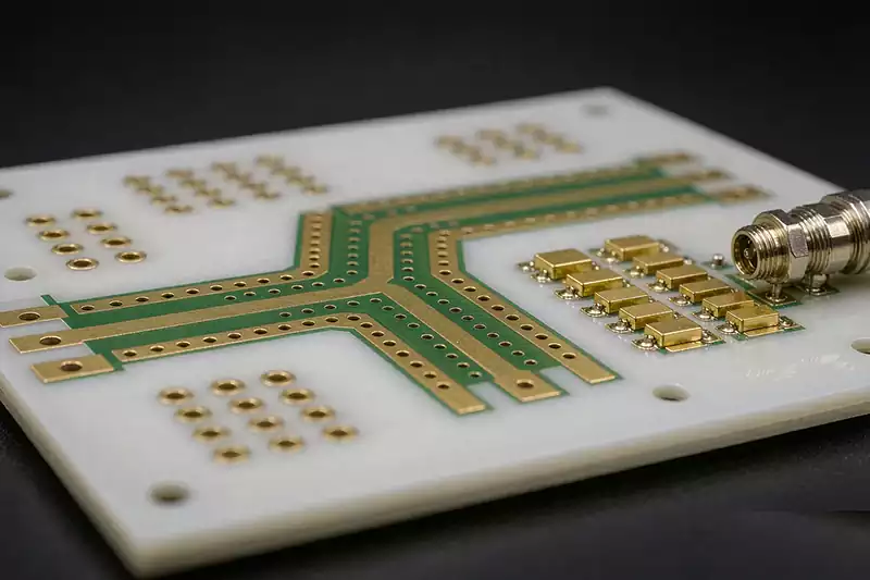
Microwave RF PCB Stackup Design Guidelines
Microwave RF PCBs commonly use multilayer stackups ranging from approximately 4 to 12 layers, depending on circuit complexity, routing density, RF architecture, and mechanical requirements.
The fundamental stackup design principle is to separate functional layers according to their electrical requirements while balancing RF performance, manufacturability, reliability, and cost.
Dedicated low-loss, high-stability RF laminates should be used for critical high-frequency signal layers. FR-4 or other cost-effective materials may be used in supporting layers for power distribution, control circuitry, or other functions that do not require the same level of high-frequency performance.
A hybrid multilayer stackup can reduce the cost associated with using high-frequency laminate throughout the entire PCB while maintaining the required electrical performance on critical RF signal paths.
The stackup should also be designed with structural symmetry and balanced material distribution whenever possible. A balanced construction helps control mechanical stress, warpage, and dimensional instability during PCB fabrication and assembly.
Key Manufacturing Requirements for Microwave RF PCBs
The production yield and long-term quality consistency of microwave RF PCBs do not depend solely on advanced manufacturing equipment. They rely on systematic control of material selection, stackup construction, impedance requirements, conductor geometry, drilling, lamination, plating, and RF-specific fabrication processes.
Five major factors have a direct impact on production performance:
High-frequency laminate grade and electrical properties
PCB layer count and stackup configuration
Controlled-impedance tolerance
Copper foil profile and surface roughness
Specialized fabrication processes for RF materials such as PTFE-based laminates
Successful volume production requires a comprehensive process-control system. The laminate grade should be selected according to the operating frequency, insertion-loss budget, thermal requirements, and mechanical constraints of the application.
The multilayer stackup should be optimized for structural balance, controlled impedance, signal integrity, and electromagnetic isolation. Tight dimensional and impedance tolerances should be defined during the engineering stage, while design-for-manufacturing (DFM) review should be completed before production.
A comprehensive DFM review can identify potential issues such as trace-width variation, via-related discontinuities, inadequate reference-plane structures, impedance mismatch, and fabrication tolerances before the design enters mass production. Addressing these issues at the engineering stage can reduce PCB redesigns and improve first-pass production yield.
A properly designed and manufactured microwave RF PCB should undergo controlled-impedance verification and appropriate RF performance testing. TDR testing can verify transmission-line impedance, while VNA measurements can characterize high-frequency parameters such as insertion loss and return loss.
With appropriate material selection, controlled stackup design, precise RF routing, impedance control, and standardized manufacturing processes, microwave RF PCBs can achieve stable and repeatable electrical performance across production lots. These capabilities make them suitable for demanding applications including 5G communication infrastructure, satellite communication, automotive millimeter-wave radar, phased-array antennas, and precision RF test and measurement equipment.