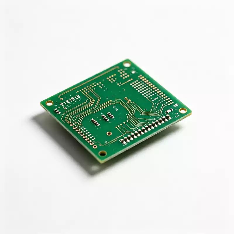
An RF PCB is a printed circuit board built to carry radio frequency and microwave signals, typically from a few hundred megahertz up to several gigahertz and beyond. At those frequencies the board stops behaving like a passive connector between components and starts acting as part of the circuit itself. That single fact is what separates an RF PCB from the ordinary digital board sitting inside a toaster or a keyboard.
Most pcb boards you encounter every day move low speed signals where a trace is just a wire. The circuit board has to treat every trace as a transmission line, because once the signal wavelength gets close to the board dimensions, reflections, losses, and coupling start to dominate. If you are sourcing or designing one, the questions are less about “will it connect” and more about “will it stay clean at the frequency it has to run.”
What is an RF PCB?
Radio frequency printed circuit boards carry signals in the RF and microwave bands used by wireless communication, radar, and high speed test equipment. The boundary is not a hard number, but a useful rule is that once your operating frequency climbs past roughly 500 MHz to 1 GHz, the layout and material decisions that digital designers can ignore become the main drivers of whether the product works.
A radio frequency PCB can be a simple two layer antenna feed or a complex multilayer stack with embedded RF, mixed signal, and digital sections on the same substrate. The common thread is that the signal integrity of the high frequency path decides the outcome, not the logic function.
Why an RF PCB is harder than a standard board
On a normal board, a small amount of loss or a tiny reflection is invisible. On a RF PCB those same imperfections eat into the link budget and show up as reduced range, higher bit error, phase noise, or spurious emissions.
Three effects do most of the damage. Dielectric loss comes from the insulating material converting part of the signal into heat, and it grows with frequency. Conductor loss grows because current crowds into the outer skin of the trace, a behavior called the skin effect. Impedance discontinuity happens wherever the trace width, height above ground, or nearby material changes, sending part of the signal back toward the source. Add crosstalk between adjacent lines and radiated emissions, and you have a board where the substrate is as important as the schematic.
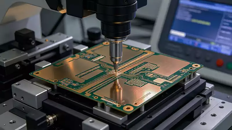
Where material choice decides signal quality
Standard FR4 is perfectly good for countless products, but it was not made for RF. Its dielectric constant drifts with frequency and temperature, and its dissipation factor is higher than what clean RF wants. The result is unpredictable impedance and avoidable loss.
RF grade laminates fix this. Materials built on PTFE, ceramic filled hydrocarbon, or similar formulations hold a stable dielectric constant and a very low dissipation factor across temperature and frequency. Rohacell style foams and Rogers laminates are common names in this space, and the trade is straightforward: better electrical behavior, higher cost, and tighter machining requirements.
When the frequency is low or the path is short, FR4 may still be fine. When the path is long, the frequency is high, or the spec leaves no margin, the material decision is the difference between a board that passes and one that needs a respin. You can read more in our notes on high frequency PCB construction and the advantages of Rogers materials in high frequency applications.
Controlled impedance is not optional
For RF work, impedance is a design parameter, not an accident. The most common targets are 50 ohms single ended, 75 ohms for some video and cable interfaces, and 100 ohms differential for high speed pairs. The geometry that delivers it is usually a microstrip (trace over a ground plane) or a stripline (trace buried between two ground planes).
The catch is tolerance. A target of 50 ohms is meaningless if the finished board lands at 60. RF work often calls for plus or minus 10 percent or tighter, which pushes the manufacturer on dielectric thickness, etch control, and material consistency. Our write up on PCB impedance covers how stack up and trace geometry set the number.
Layout rules that protect the signal
Good RF layout is mostly discipline. Keep a solid, unbroken reference ground plane under the RF path so the return current has a short, predictable route. Keep RF traces as short as the package allows and route them away from noisy digital or power sections. Avoid stubs, because an open branch is an antenna and a mismatch. Watch via placement, since every via adds parasitic inductance that matters more as frequency rises. Where isolation is tight, a coplanar waveguide with ground on both sides of the trace helps keep energy where it belongs.
None of these rules are exotic. They are the difference between a layout drawn once and a layout drawn three times.
Surface finish and manufacturing tolerance
The finish on the exposed pads matters more at RF than at DC. Hot air solder leveling leaves an uneven surface that adds loss and variability, so ENIG (electroless nickel immersion gold) is the usual choice for RF pads: flat, stable, and consistent. Immersion silver is another option where the application allows it.
Manufacturing tolerance is the quiet hero. Tighter etch control keeps trace impedance on target, uniform plating keeps insertion loss predictable, and filled or capped vias keep RF transitions clean. A board that looks identical on the screen can behave very differently on the bench depending on how tightly these are held.
Where RF PCBs end up
If a device sends or receives at high frequency, there is probably an RF PCB inside it. Cellular and 5G infrastructure, Wi Fi and Bluetooth modules, automotive radar, aerospace and satellite systems, medical imaging, and laboratory test equipment all rely on boards built to these rules. The Internet of Things pushed RF into countless small, cost sensitive products, which is exactly where the material versus budget trade off gets argued most often.
What to put on the purchase order
When you ask a factory to build this kind of board, vague drawings invite vague results. State the operating frequency band, the target impedance values with their tolerances, and the laminate you need or a clear rule for substitution. Give the layer count and stack up, the surface finish, and any RF specific inspection or test you expect, such as impedance coupon measurement or insertion loss checks on critical lines.
For the deeper engineering side, our microwave RF PCB design and manufacturing guidelines go further into stack up and process choices.
Frequently asked questions about RF PCBs
What frequency makes a board an RF PCB?
There is no hard cutoff. A useful rule is that once the operating frequency rises past roughly 500 MHz to 1 GHz, transmission line effects, loss, and coupling start to dominate, and the board has to be treated as an RF PCB rather than an ordinary digital board.
Can standard FR4 be used for radio frequency boards?
Often yes, for lower frequencies or short, non critical paths. FR4 works, but its dielectric constant shifts with frequency and temperature and its dissipation factor is higher than RF grade laminates. As frequency climbs or margin shrinks, a stable low loss material becomes the safer choice.
What impedance do radio frequency boards use?
The common targets are 50 ohms single ended, 75 ohms for some interfaces, and 100 ohms differential for high speed pairs. The value is set by trace geometry over a ground plane, and RF work usually demands a tight tolerance such as plus or minus 10 percent.
Which surface finish is best for radio frequency boards?
ENIG, electroless nickel immersion gold, is the usual pick because it is flat and stable and does not add the loss and variation that hot air solder leveling can introduce. Immersion silver is another option where the application allows it.
What should I write when ordering an RF PCB?
State the frequency band, the target impedance values with tolerances, the laminate or a clear substitution rule, the layer count and stack up, the surface finish, and any RF specific inspection such as impedance coupons or insertion loss checks on critical lines.
An RF PCB rewards teams that treat the substrate as a circuit element instead of a backing sheet. Pick the material for the frequency, lock the impedance with intent, and lay the paths out so the signal returns home cleanly. Do those three things and the board you receive will behave like the one you simulated, which is the whole point of building an RF PCB in the first place.